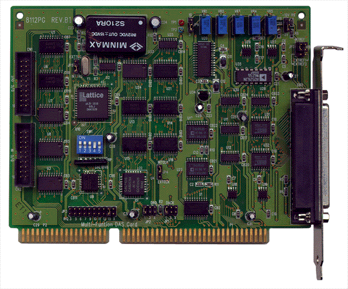
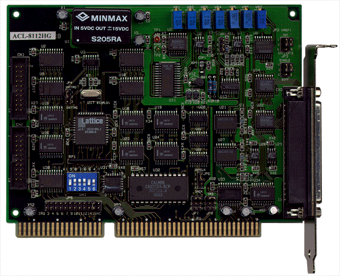
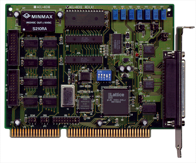
Comprehensive Product Summary – ADLINK ACL‑8312 Data Acquisition Card
### 1. Product Overview
Product Name: ACL‑8312
Model: ACL‑8312
Series: ACL‑8316/8312 High‑Performance DAS (Data Acquisition System) Cards
Article Number: ACL‑8312
Manufacturer: ADLINK Technology Inc.
Trademark: NuDAQ® Series
Product Description:
The ADLINK ACL‑8312 is a high‑performance, 12‑bit analog‑to‑digital (A/D) and digital‑to‑analog (D/A) data acquisition card designed for PC/ISA bus systems. It provides 16 single‑ended or 8 differential analog input channels, two 12‑bit analog output channels, 16 digital I/O lines, and three programmable 16‑bit counters. With a maximum sampling rate of 100 kS/s and a 1 K‑word FIFO buffer, the ACL‑8312 is optimized for continuous, gap‑free data acquisition in industrial, laboratory, and control applications.
### 2. Key Features
- High‑Speed A/D Conversion:
12‑bit successive‑approximation ADC (ADS7804 or equivalent) with up to 100 kHz sampling rate.
- Flexible Analog Input Configuration:
16 single‑ended or 8 differential channels with programmable gain (×1, ×2, ×4, ×8) and bipolar input ranges of ±10 V, ±5 V, ±2.5 V, or ±1.25 V.
- On‑Board FIFO Buffer:
1 K‑word FIFO memory for gap‑free, high‑speed data acquisition with half‑full and full interrupt flags.
- Dual 12‑bit D/A Outputs:
Two independent DAC2813 (or equivalent) channels, ±10 V or 0–10 V output range, 6 µs settling time, ±5 mA drive.
- Digital I/O:
16 TTL‑compatible digital input/output lines for control and monitoring.
- Programmable Counter/Timer:
Intel 8254‑compatible 3×16‑bit counters with 2 MHz base clock; supports pacer triggering and event counting.
- DMA and Interrupt Support:
Supports DMA channels 5, 6, 7 and IRQ levels 3, 5–7, 9, 11, 12, 15 for efficient data transfer.
- Auto‑Scanning and Triggering:
Software, internal pacer, or external trigger modes; automatic channel scanning for sequential sampling.
- Integrated DC/DC Converter:
Provides stable analog power isolation from digital circuitry.
- Compact Half‑Size ISA Form Factor:
163 mm × 123 mm PCB with 37‑pin D‑type and dual 20‑pin IDC connectors.
- Software Support:
Includes DOS C/C++ library, Windows DLL (ACLS‑DLL2), and LabVIEW driver (ACLS‑LVIEW).
### 3. Technical Specifications
Analog Input (A/D):
- Converter: ADS7804 (12‑bit successive approximation)
- Channels: 16 SE or 8 DI
- Resolution: 12 bits
- Conversion Time: 8 µs
- Max Sampling Rate: 100 kS/s
- Input Range (programmable): ±10 V, ±5 V, ±2.5 V, ±1.25 V
- Input Impedance: 10 MΩ
- Accuracy:
- Gain = 1: 0.01 % FSR ± 1 LSB
- Gain = 2, 4: 0.02 % FSR ± 1 LSB
- Gain = 8: 0.04 % FSR ± 1 LSB
- Over‑Voltage Protection: ±35 V continuous
- Data Format: Two’s complement
- FIFO Buffer: 1 K words with half/full interrupt
- Trigger Modes: Software, internal pacer, external pulse
- Data Transfer: Polling, interrupt, FIFO, or DMA
Analog Output (D/A):
- Converter: DAC2813 or equivalent
- Channels: 2
- Resolution: 12 bits
- Output Range: ±10 V (bipolar) or 0–10 V (unipolar)
- Settling Time: 4.5 µs typ., 6 µs max
- Output Drive: ±5 mA min
- Output Impedance: 0.2 Ω
- Linearity: ±½ LSB max
- Modes: Double‑buffered or transparent
- Data Format: Binary or two’s complement
Digital I/O:
- Channels: 16 TTL‑compatible (input/output)
- Input Voltage: Low ≤ 0.8 V, High ≥ 2.0 V
- Output Voltage: Low ≤ 0.4 V, High ≥ 2.4 V
- Drive Capability: Sink 8 mA @ 0.5 V, Source 0.4 mA @ 2.7 V
Programmable Counter/Timer:
- Device: Intel 82C54
- Counters: 3 × 16‑bit (2 MHz base)
- Pacer Output: 0.00046 Hz – 100 kHz
- Modes: 0–5 (interrupt, one‑shot, rate generator, square wave, strobe)
- External Clock Input: CN3 pin 37
General:
- Bus Interface: 16‑bit ISA
- I/O Base Address: 16 consecutive locations (200h–3FFh)
- IRQ Levels: 3, 5, 6, 7, 9, 11, 12, 15
- DMA Channels: 5, 6, 7
- Power Requirements: +5 V @ 400 mA typ., +12 V @ 260 mA typ.
- Operating Temperature: 0 °C – 55 °C
- Storage Temperature: −20 °C – 80 °C
- Humidity: 5 – 95 % non‑condensing
- Dimensions: 163 mm (L) × 123 mm (H)
- Connectors:
- CN3: 37‑pin D‑type (analog I/O, timer)
- CN1/CN2: 2 × 20‑pin IDC (digital I/O)
### 4. Functionality
Operation Principle:
The ACL‑8312 performs analog‑to‑digital conversion using a 12‑bit successive‑approximation ADC. Input signals are multiplexed across 16 SE or 8 DI channels, amplified by a programmable gain amplifier, and digitized at up to 100 kS/s. Data is buffered in a 1 K FIFO and transferred to system memory via polling, interrupt, or DMA.
Use Cases:
- Industrial process monitoring and control
- Laboratory data logging and signal analysis
- Energy management and automation
- Product testing and quality assurance
- Security and annunciation systems
- Pulse width and frequency measurement
Compatibility:
ISA‑bus PCs running DOS, Windows 95/98/NT. Supported by ADLINK’s NuDAQ software suite, C/C++ libraries, and LabVIEW drivers.
### 5. Components & Accessories
Included:
- ACL‑8312 Data Acquisition Card
- ADLINK Software CD (utilities, drivers, libraries)
- User’s Manual
Optional Daughter Boards:
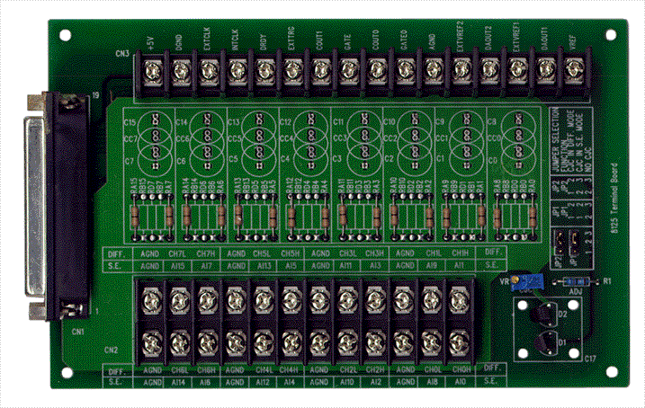
- ACLD‑8125: 37‑pin terminal board with cold‑junction compensation for thermocouples.
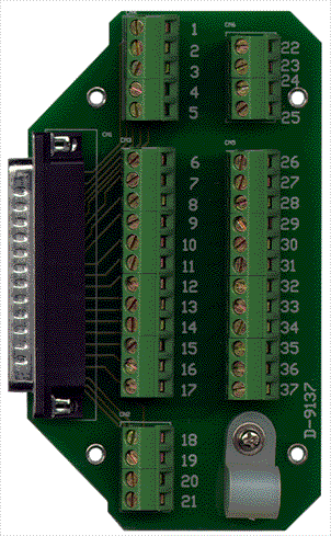
- ACLD‑9137: Direct 37‑pin connector board for simple wiring.
- ACLD‑9182: 16‑channel isolated digital input board (500 V DC isolation).
- ACLD‑9185: 16‑channel SPDT relay output board.
- ACLD‑9188 / 9138: General‑purpose terminal boards (barrier‑strip or screw‑clamp).
Connectors:
- CN3 (37‑pin D‑type): Analog inputs/outputs, counter/timer, external trigger/clock.
- CN1 (20‑pin IDC): Digital outputs (DO 0–15).
- CN2 (20‑pin IDC): Digital inputs (DI 0–15).
### 6. Installation & Setup
Requirements:
- IBM‑compatible PC with available 16‑bit ISA slot.
- DOS or Windows 95/98/NT operating system.
- Anti‑static handling precautions during installation.
Configuration:
- Base Address: Set via 6‑position DIP switch (SW1); default = 220h.
- Analog Input Mode: JP7 selects 16 SE or 8 DI.
- Analog Output Range: JP5 (CH1) and JP6 (CH2) select ±10 V (bipolar) or 0–10 V (unipolar).
- Output Mode: JP8 selects double‑buffered or transparent.
- DMA Channel: JP1/JP2 select DMA 5, 6, or 7.
- IRQ Level: JP3 selects IRQ 3, 5–7, 9, 11, 12, 15 (default = 15).
- Clock Source: JP4 selects internal 2 MHz (default) or external (CN3 pin 37).
Software Installation:
- DOS utilities and C/C++ library via ADLINK CD.
- Windows drivers (ACLS‑DLL2) and LabVIEW VIs (ACLS‑LVIEW) included.
### 7. Performance & Capabilities
- A/D Sampling Rate: Up to 100 kS/s continuous.
- FIFO Buffer: 1 K samples (≈ 10 ms at 100 kS/s).
- A/D Conversion Time: 8 µs.
- D/A Settling Time: ≤ 6 µs.
- Timer Resolution: 2 MHz base, 0.5 µs tick.
- DMA Throughput: Real‑time, CPU‑independent transfer.
- Accuracy: ±0.01 % FSR (typical gain 1).
- Input Protection: ±35 V continuous.
- Output Drive: ±5 mA per channel.
- Limitations: ISA bus bandwidth; FIFO depth 1 K samples; no simultaneous sampling across channels.
### 8. Standards & Compliance
- Bus Interface: 16‑bit ISA (AT bus)
- Timer/Counter: Intel 8254 compatible
- DMA Controller: 8237 compatible
- Interrupts: PC/AT IRQ standard
- Digital Logic: TTL/DTL compatible I/O
- Environmental: Operating 0–55 °C, Storage −20–80 °C, Humidity 5–95 % non‑condensing
- Safety & Quality: Manufactured to ADLINK industrial standards; meets typical EMC and safety requirements for ISA cards of its class.
### 9. Additional Information
Calibration:
- Adjustable VR potentiometers for A/D and D/A offset and gain:
- VR1 A/D offset, VR2 A/D full‑scale, VR3–VR6 D/A channel calibration, VR7 PGA offset.
- Calibration procedure uses precision multimeter and voltage source; software utility included.
Software Support:
- DOS C/C++ library with 28 API functions for A/D, D/A, DIO, and timer control.
- Windows DLL (ACLS‑DLL2) for VC++, VB, Delphi.
- LabVIEW driver (ACLS‑LVIEW) for graphical programming.
- Utility programs for configuration, testing, and calibration.
Warranty:
- 1‑year limited warranty against defects in materials and workmanship.
- Excludes damage from misuse, modification, or operation beyond specifications.
- Return requires RMA and proof of purchase; customer pays shipping.
Support & Contact:
- ADLINK Technology Inc.
9F, No. 166, Jian Yi Road, Chungho City, Taipei 235, Taiwan R.O.C.
Tel: +886‑2‑8226‑5877 Fax: +886‑2‑8226‑5717
Web: [www.adlink.com.tw](http://www.adlink.com.tw)
Email: service@adlink.com.tw | nudaq@adlink.com.tw
Maintenance:
- Periodic calibration recommended for accuracy.
- Keep card free from dust and static discharge.
- Firmware and software updates available via ADLINK support.
### Summary
The ADLINK ACL‑8312 is a robust, high‑precision, multifunction data acquisition card engineered for ISA‑bus PCs. It combines 12‑bit analog input and output, digital I/O, and timing functions into a compact, reliable platform. With its 100 kS/s sampling rate, 1 K FIFO buffer, and flexible triggering and DMA capabilities, it supports demanding real‑time measurement and control tasks. Comprehensive software libraries and calibration utilities make it suitable for both OEM integration and laboratory research environments.

 SUCHEN SIE DIE PASSENDE
 A8316&12 Manual.PDF
Manual
A8316&12 Manual.PDF
Manual