WD-DASK
SUCHEN SIE DIE PASSENDE
INDUSTRIELLE LÖSUNG?
Entdecken Sie Embedded-, Kommunikations- und Automatisierungslösungen für Ihre Anwendung.
- High-Speed Sampling: Up to 200 MS/s per channel simultaneous sampling.
- High Resolution: 14-bit analog-to-digital conversion for precise signal representation.
- Wide Bandwidth: 90 MHz (-3 dB) analog input bandwidth for high-frequency signals.
- Flexible Input Ranges: Programmable ±0.2 V, ±2 V, or ±10 V input voltage ranges.
- Dual Analog Inputs: Two single-ended channels with software-selectable 50 Ω or 1 MΩ impedance.
- Large Onboard Memory: 1 GB acquisition memory shared between channels.
- High-Speed Data Streaming: Continuous data transfer up to 800 MB/s using scatter-gather DMA.
- Triggering Options: Software, external digital, analog, and SSI (System Synchronized Interface) triggers.
- Multiple Trigger Modes: Post-trigger, pre-trigger, middle-trigger, delayed-trigger, and re-trigger modes.
- Signal Averaging: Onboard signal averaging for noise reduction and small-signal detection.
- Auto-Calibration: Fully automatic calibration with onboard reference voltages (+5 V and +2.5 V).
- External Clocking: Supports internal 200 MHz clock or external clock input (40–200 MHz).
- Synchronization: SSI interface for multi-card synchronization (ACL-eSSI-2/3/4 cables).
- Software Compatibility: Supports LabVIEW, MATLAB, Visual Studio, and ADLINK’s DAQPilot SDK.
- Operating Systems: Windows XP/7/8 (x86/x64).
- Compliance: CE and FCC Class A certified; RoHS and WEEE compliant.
- High Resolution: 14-bit analog-to-digital conversion for precise signal representation.
- Wide Bandwidth: 90 MHz (-3 dB) analog input bandwidth for high-frequency signals.
- Flexible Input Ranges: Programmable ±0.2 V, ±2 V, or ±10 V input voltage ranges.
- Dual Analog Inputs: Two single-ended channels with software-selectable 50 Ω or 1 MΩ impedance.
- Large Onboard Memory: 1 GB acquisition memory shared between channels.
- High-Speed Data Streaming: Continuous data transfer up to 800 MB/s using scatter-gather DMA.
- Triggering Options: Software, external digital, analog, and SSI (System Synchronized Interface) triggers.
- Multiple Trigger Modes: Post-trigger, pre-trigger, middle-trigger, delayed-trigger, and re-trigger modes.
- Signal Averaging: Onboard signal averaging for noise reduction and small-signal detection.
- Auto-Calibration: Fully automatic calibration with onboard reference voltages (+5 V and +2.5 V).
- External Clocking: Supports internal 200 MHz clock or external clock input (40–200 MHz).
- Synchronization: SSI interface for multi-card synchronization (ACL-eSSI-2/3/4 cables).
- Software Compatibility: Supports LabVIEW, MATLAB, Visual Studio, and ADLINK’s DAQPilot SDK.
- Operating Systems: Windows XP/7/8 (x86/x64).
- Compliance: CE and FCC Class A certified; RoHS and WEEE compliant.
Comprehensive Product Summary: ADLINK PCIe-9852 High-Speed PCI Express Digitizer
### 1. Product Overview
Product Name: PCIe-9852
Model: PCIe-9852
Series: PCI Express High-Speed Digitizer Series
Article Number: 50-11041-1000
Manufacturer: ADLINK Technology, Inc.
Product Type: 2-Channel 14-Bit 200 MS/s PCI Express Analog-to-Digital (A/D) Conversion Card
Form Factor: PCI Express Gen 2 x4 plug-in card
Dimensions: 167.64 mm (W) × 106.68 mm (H) (6.53” × 4.16”)
Revision: Manual Rev. 2.00 (May 20, 2013)
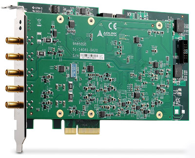
The ADLINK PCIe-9852 is a high-performance, two-channel, 14-bit, 200 mega-samples per second (MS/s) digitizer designed for high-frequency, wide dynamic range signal acquisition. It integrates a PCI Express Gen 2 x4 interface, 1 GB onboard memory, and advanced triggering and synchronization features, making it suitable for demanding applications such as optical fiber testing, LIDAR, radar signal analysis, and high-speed data acquisition in research and industrial environments.
### 2. Key Features
- High-Speed Sampling: Up to 200 MS/s per channel simultaneous sampling.
- High Resolution: 14-bit analog-to-digital conversion for precise signal representation.
- Wide Bandwidth: 90 MHz (-3 dB) analog input bandwidth for high-frequency signals.
- Flexible Input Ranges: Programmable ±0.2 V, ±2 V, or ±10 V input voltage ranges.
- Dual Analog Inputs: Two single-ended channels with software-selectable 50 Ω or 1 MΩ impedance.
- Large Onboard Memory: 1 GB acquisition memory shared between channels.
- High-Speed Data Streaming: Continuous data transfer up to 800 MB/s using scatter-gather DMA.
- Triggering Options: Software, external digital, analog, and SSI (System Synchronized Interface) triggers.
- Multiple Trigger Modes: Post-trigger, pre-trigger, middle-trigger, delayed-trigger, and re-trigger modes.
- Signal Averaging: Onboard signal averaging for noise reduction and small-signal detection.
- Auto-Calibration: Fully automatic calibration with onboard reference voltages (+5 V and +2.5 V).
- External Clocking: Supports internal 200 MHz clock or external clock input (40–200 MHz).
- Synchronization: SSI interface for multi-card synchronization (ACL-eSSI-2/3/4 cables).
- Software Compatibility: Supports LabVIEW, MATLAB, Visual Studio, and ADLINK’s DAQPilot SDK.
- Operating Systems: Windows XP/7/8 (x86/x64).
- Compliance: CE and FCC Class A certified; RoHS and WEEE compliant.
### 3. Technical Specifications
Analog Input:
- Channels: 2 single-ended
- Connector Type: SMA
- Input Coupling: AC or DC (software selectable)
- AC Coupling Cutoff Frequency: 11 Hz
- Input Impedance: 50 Ω or 1 MΩ (software selectable)
- Input Voltage Ranges: ±0.2 V, ±2 V, ±10 V
- Bandwidth: 90 MHz (-3 dB)
- ADC Resolution: 14 bits (1 in 16,384)
- Gain Error: ±0.65%
- Offset Error: ±1 mV
- Crosstalk: < -80 dB
- Overvoltage Protection: ±10 V sine wave (7 Vrms) for 50 Ω; ±10 V for 1 MΩ
Spectral Performance (200 MS/s):
- ±0.2 V Range: SINAD 61.72 dBc, SNR 61.77 dBc, THD -81.42 dBc, ENOB 9.96 bits, SFDR 82.75 dBc
- ±2 V Range: SINAD 62.06 dBc, SNR 62.11 dBc, THD -80.97 dBc, ENOB 10.02 bits, SFDR 85.87 dBc
Trigger System:
- Sources: Software, external digital, analog, SSI
- Modes: Post, pre, middle, delayed, re-trigger
- External Trigger Input: SMA, 3.3 V TTL (5 V tolerant), 20 ns min pulse width
- External Trigger Output: SMA, 5 V TTL, programmable pulse width (50 ns–10 μs), drives 50 Ω load
Timebase:
- Internal Clock: 200 MHz synthesizer
- External Clock Input: 40–200 MHz (1 Vpp–5 Vpp)
- External Reference Clock: 10 MHz (500 mVpp–5 Vpp)
- Timebase Accuracy: ±25 ppm
- Warm-Up Time: 15 minutes
Data Storage and Transfer:
- Onboard Memory: 1 GB shared
- Transfer Mode: Scatter-gather DMA
- Continuous Streaming: Up to 800 MB/s
Power Requirements:
| Power Rail | Standby (mA) | Full Load (mA) |
|-------------|--------------|----------------|
| +3.3 V | 102 | 102.2 |
| +12 V | 20 | 20 |
| +5 V | 1920 | 2010 |
Environmental:
- Operating Temperature: 0°C to 50°C
- Storage Temperature: -20°C to 80°C
- Humidity: 10–90% non-condensing
Physical:
- Dimensions: 167.64 mm × 106.68 mm
- Connectors: 5 SMA (CH0, CH1, TRG IN, TRG OUT, CLK IN)
- Bus Interface: PCI Express Gen 2 x4
### 4. Functionality
The PCIe-9852 digitizer converts analog signals into high-resolution digital data for analysis and processing. Each of the two channels can simultaneously sample at up to 200 MS/s, capturing fast transient signals with high fidelity. The card’s FPGA-based architecture manages data acquisition, triggering, and DMA transfer to host memory.
Use Cases:
- Optical fiber and LIDAR testing
- Radar and RF signal acquisition
- Video IC and high-speed electronics testing
- Distributed temperature sensing (DTS)
- Physics and research laboratories
- Power system diagnostics (partial discharge monitoring)
Compatibility:
- Works with Windows XP/7/8 (x86/x64)
- Compatible with LabVIEW, MATLAB, Visual Studio, and ADLINK DAQPilot SDK
### 5. Components & Accessories
Included Items:
- PCIe-9852 digitizer card
- ADLINK All-in-One software CD
- Quick Start Guide
Optional Accessories:
- ACL-eSSI-2/3/4: SSI bus cables for synchronization of 2, 3, or 4 modules
- SMA Cables: For analog input, trigger, and clock connections
Front Panel Connectors:
- CH0, CH1: Analog inputs (SMA)
- TRG IN: External trigger input (SMA)
- TRG OUT: External trigger output (SMA)
- CLK IN: External clock input (SMA)
### 6. Installation & Setup
Requirements:
- Available PCI Express x4 slot (Gen 2 compliant)
- Anti-static precautions during installation
- Compatible host PC running supported OS
Installation Steps:
1. Power off the host system and remove the cover.
2. Insert the PCIe-9852 into an available PCIe x4 slot.
3. Secure the bracket with the retaining screw.
4. Replace the cover and power on the system.
5. Install drivers and software from the ADLINK All-in-One CD.
Configuration:
- Input coupling, impedance, and voltage range are software-selectable.
- Trigger and clock sources can be configured via software.
- Multi-card synchronization via SSI interface and ACL-eSSI cables.
### 7. Performance & Capabilities
Sampling Rate: Up to 200 MS/s per channel
Resolution: 14 bits
Bandwidth: 90 MHz (-3 dB)
Data Throughput: Up to 800 MB/s continuous streaming
Memory: 1 GB onboard
Dynamic Range: ENOB up to 10.02 bits
Signal Averaging: Hardware-based averaging for noise reduction
Trigger Latency: <20 ns (digital trigger)
Synchronization: Multi-module synchronization via SSI bus
Limitations:
- Maximum external clock frequency: 200 MHz
- Input voltage limited to ±10 V
- Operating temperature limited to 50°C
### 8. Standards & Compliance
Certifications:
- CE (Electromagnetic Compatibility)
- FCC Class A (EMI/EMC)
Environmental Compliance:
- RoHS (Restriction of Hazardous Substances)
- WEEE (Waste Electrical and Electronic Equipment)
Bus Interface Standard:
- PCI Express Specification Revision 2.0 compliant
Safety:
- Designed for operation in non-condensing environments
- Requires anti-static handling precautions
### 9. Additional Information
Calibration:
- Factory-calibrated with constants stored in EEPROM (Bank 0).
- User auto-calibration supported (Bank 1).
- Onboard reference voltages: +5 V and +2.5 V with <3 ppm/°C drift.
- Recommended warm-up: 15–20 minutes before calibration.
Warranty & Support:
- Manufacturer: ADLINK Technology, Inc.
- Global support network with offices in Taiwan, USA, China, Japan, Germany, France, Korea, Singapore, India, and Israel.
- Technical support via email: service@adlinktech.com
Maintenance:
- Periodic recalibration recommended for long-term accuracy.
- Avoid exposure to moisture, dust, and electrostatic discharge.
Software & Drivers:
- DAQPilot SDK: For VB.NET, VC++, Delphi, and LabVIEW.
- WD-DASK Driver: For Windows XP/7/8, binary compatible across versions.
- MATLAB Toolbox Adapter: For direct integration with MATLAB environments.
Environmental Responsibility:
ADLINK adheres to RoHS and WEEE directives, ensuring environmentally responsible manufacturing and disposal practices.
### Summary
The ADLINK PCIe-9852 is a robust, high-speed, dual-channel digitizer optimized for precision data acquisition in high-frequency applications. With a 14-bit resolution, 200 MS/s sampling rate, and 90 MHz bandwidth, it delivers exceptional accuracy and dynamic performance. Its PCI Express Gen 2 x4 interface ensures high-throughput data streaming, while the 1 GB onboard memory supports extended acquisition sessions. The card’s flexible triggering, synchronization, and clocking options make it ideal for complex test and measurement setups. Combined with comprehensive software support and compliance with international standards, the PCIe-9852 stands as a versatile and reliable solution for advanced signal digitization and analysis.

### 1. Product Overview
Product Name: PCIe-9852
Model: PCIe-9852
Series: PCI Express High-Speed Digitizer Series
Article Number: 50-11041-1000
Manufacturer: ADLINK Technology, Inc.
Product Type: 2-Channel 14-Bit 200 MS/s PCI Express Analog-to-Digital (A/D) Conversion Card
Form Factor: PCI Express Gen 2 x4 plug-in card
Dimensions: 167.64 mm (W) × 106.68 mm (H) (6.53” × 4.16”)
Revision: Manual Rev. 2.00 (May 20, 2013)
The ADLINK PCIe-9852 is a high-performance, two-channel, 14-bit, 200 mega-samples per second (MS/s) digitizer designed for high-frequency, wide dynamic range signal acquisition. It integrates a PCI Express Gen 2 x4 interface, 1 GB onboard memory, and advanced triggering and synchronization features, making it suitable for demanding applications such as optical fiber testing, LIDAR, radar signal analysis, and high-speed data acquisition in research and industrial environments.
### 2. Key Features
- High-Speed Sampling: Up to 200 MS/s per channel simultaneous sampling.
- High Resolution: 14-bit analog-to-digital conversion for precise signal representation.
- Wide Bandwidth: 90 MHz (-3 dB) analog input bandwidth for high-frequency signals.
- Flexible Input Ranges: Programmable ±0.2 V, ±2 V, or ±10 V input voltage ranges.
- Dual Analog Inputs: Two single-ended channels with software-selectable 50 Ω or 1 MΩ impedance.
- Large Onboard Memory: 1 GB acquisition memory shared between channels.
- High-Speed Data Streaming: Continuous data transfer up to 800 MB/s using scatter-gather DMA.
- Triggering Options: Software, external digital, analog, and SSI (System Synchronized Interface) triggers.
- Multiple Trigger Modes: Post-trigger, pre-trigger, middle-trigger, delayed-trigger, and re-trigger modes.
- Signal Averaging: Onboard signal averaging for noise reduction and small-signal detection.
- Auto-Calibration: Fully automatic calibration with onboard reference voltages (+5 V and +2.5 V).
- External Clocking: Supports internal 200 MHz clock or external clock input (40–200 MHz).
- Synchronization: SSI interface for multi-card synchronization (ACL-eSSI-2/3/4 cables).
- Software Compatibility: Supports LabVIEW, MATLAB, Visual Studio, and ADLINK’s DAQPilot SDK.
- Operating Systems: Windows XP/7/8 (x86/x64).
- Compliance: CE and FCC Class A certified; RoHS and WEEE compliant.
### 3. Technical Specifications
Analog Input:
- Channels: 2 single-ended
- Connector Type: SMA
- Input Coupling: AC or DC (software selectable)
- AC Coupling Cutoff Frequency: 11 Hz
- Input Impedance: 50 Ω or 1 MΩ (software selectable)
- Input Voltage Ranges: ±0.2 V, ±2 V, ±10 V
- Bandwidth: 90 MHz (-3 dB)
- ADC Resolution: 14 bits (1 in 16,384)
- Gain Error: ±0.65%
- Offset Error: ±1 mV
- Crosstalk: < -80 dB
- Overvoltage Protection: ±10 V sine wave (7 Vrms) for 50 Ω; ±10 V for 1 MΩ
Spectral Performance (200 MS/s):
- ±0.2 V Range: SINAD 61.72 dBc, SNR 61.77 dBc, THD -81.42 dBc, ENOB 9.96 bits, SFDR 82.75 dBc
- ±2 V Range: SINAD 62.06 dBc, SNR 62.11 dBc, THD -80.97 dBc, ENOB 10.02 bits, SFDR 85.87 dBc
Trigger System:
- Sources: Software, external digital, analog, SSI
- Modes: Post, pre, middle, delayed, re-trigger
- External Trigger Input: SMA, 3.3 V TTL (5 V tolerant), 20 ns min pulse width
- External Trigger Output: SMA, 5 V TTL, programmable pulse width (50 ns–10 μs), drives 50 Ω load
Timebase:
- Internal Clock: 200 MHz synthesizer
- External Clock Input: 40–200 MHz (1 Vpp–5 Vpp)
- External Reference Clock: 10 MHz (500 mVpp–5 Vpp)
- Timebase Accuracy: ±25 ppm
- Warm-Up Time: 15 minutes
Data Storage and Transfer:
- Onboard Memory: 1 GB shared
- Transfer Mode: Scatter-gather DMA
- Continuous Streaming: Up to 800 MB/s
Power Requirements:
| Power Rail | Standby (mA) | Full Load (mA) |
|-------------|--------------|----------------|
| +3.3 V | 102 | 102.2 |
| +12 V | 20 | 20 |
| +5 V | 1920 | 2010 |
Environmental:
- Operating Temperature: 0°C to 50°C
- Storage Temperature: -20°C to 80°C
- Humidity: 10–90% non-condensing
Physical:
- Dimensions: 167.64 mm × 106.68 mm
- Connectors: 5 SMA (CH0, CH1, TRG IN, TRG OUT, CLK IN)
- Bus Interface: PCI Express Gen 2 x4
### 4. Functionality
The PCIe-9852 digitizer converts analog signals into high-resolution digital data for analysis and processing. Each of the two channels can simultaneously sample at up to 200 MS/s, capturing fast transient signals with high fidelity. The card’s FPGA-based architecture manages data acquisition, triggering, and DMA transfer to host memory.
Use Cases:
- Optical fiber and LIDAR testing
- Radar and RF signal acquisition
- Video IC and high-speed electronics testing
- Distributed temperature sensing (DTS)
- Physics and research laboratories
- Power system diagnostics (partial discharge monitoring)
Compatibility:
- Works with Windows XP/7/8 (x86/x64)
- Compatible with LabVIEW, MATLAB, Visual Studio, and ADLINK DAQPilot SDK
### 5. Components & Accessories
Included Items:
- PCIe-9852 digitizer card
- ADLINK All-in-One software CD
- Quick Start Guide
Optional Accessories:
- ACL-eSSI-2/3/4: SSI bus cables for synchronization of 2, 3, or 4 modules
- SMA Cables: For analog input, trigger, and clock connections
Front Panel Connectors:
- CH0, CH1: Analog inputs (SMA)
- TRG IN: External trigger input (SMA)
- TRG OUT: External trigger output (SMA)
- CLK IN: External clock input (SMA)
### 6. Installation & Setup
Requirements:
- Available PCI Express x4 slot (Gen 2 compliant)
- Anti-static precautions during installation
- Compatible host PC running supported OS
Installation Steps:
1. Power off the host system and remove the cover.
2. Insert the PCIe-9852 into an available PCIe x4 slot.
3. Secure the bracket with the retaining screw.
4. Replace the cover and power on the system.
5. Install drivers and software from the ADLINK All-in-One CD.
Configuration:
- Input coupling, impedance, and voltage range are software-selectable.
- Trigger and clock sources can be configured via software.
- Multi-card synchronization via SSI interface and ACL-eSSI cables.
### 7. Performance & Capabilities
Sampling Rate: Up to 200 MS/s per channel
Resolution: 14 bits
Bandwidth: 90 MHz (-3 dB)
Data Throughput: Up to 800 MB/s continuous streaming
Memory: 1 GB onboard
Dynamic Range: ENOB up to 10.02 bits
Signal Averaging: Hardware-based averaging for noise reduction
Trigger Latency: <20 ns (digital trigger)
Synchronization: Multi-module synchronization via SSI bus
Limitations:
- Maximum external clock frequency: 200 MHz
- Input voltage limited to ±10 V
- Operating temperature limited to 50°C
### 8. Standards & Compliance
Certifications:
- CE (Electromagnetic Compatibility)
- FCC Class A (EMI/EMC)
Environmental Compliance:
- RoHS (Restriction of Hazardous Substances)
- WEEE (Waste Electrical and Electronic Equipment)
Bus Interface Standard:
- PCI Express Specification Revision 2.0 compliant
Safety:
- Designed for operation in non-condensing environments
- Requires anti-static handling precautions
### 9. Additional Information
Calibration:
- Factory-calibrated with constants stored in EEPROM (Bank 0).
- User auto-calibration supported (Bank 1).
- Onboard reference voltages: +5 V and +2.5 V with <3 ppm/°C drift.
- Recommended warm-up: 15–20 minutes before calibration.
Warranty & Support:
- Manufacturer: ADLINK Technology, Inc.
- Global support network with offices in Taiwan, USA, China, Japan, Germany, France, Korea, Singapore, India, and Israel.
- Technical support via email: service@adlinktech.com
Maintenance:
- Periodic recalibration recommended for long-term accuracy.
- Avoid exposure to moisture, dust, and electrostatic discharge.
Software & Drivers:
- DAQPilot SDK: For VB.NET, VC++, Delphi, and LabVIEW.
- WD-DASK Driver: For Windows XP/7/8, binary compatible across versions.
- MATLAB Toolbox Adapter: For direct integration with MATLAB environments.
Environmental Responsibility:
ADLINK adheres to RoHS and WEEE directives, ensuring environmentally responsible manufacturing and disposal practices.
### Summary
The ADLINK PCIe-9852 is a robust, high-speed, dual-channel digitizer optimized for precision data acquisition in high-frequency applications. With a 14-bit resolution, 200 MS/s sampling rate, and 90 MHz bandwidth, it delivers exceptional accuracy and dynamic performance. Its PCI Express Gen 2 x4 interface ensures high-throughput data streaming, while the 1 GB onboard memory supports extended acquisition sessions. The card’s flexible triggering, synchronization, and clocking options make it ideal for complex test and measurement setups. Combined with comprehensive software support and compliance with international standards, the PCIe-9852 stands as a versatile and reliable solution for advanced signal digitization and analysis.
-
PCIe-9852_Datasheet_en_1.pdf
PDF Catalog

- WD-DASK - Windows driver API for PCI/PXI-9820 and PXI-98xx Digitizer
- SMB-BNC-1m - SMB to BNC cable 1m (PXI-9816/26/46)