EBC-1200
SUCHEN SIE DIE PASSENDE
INDUSTRIELLE LÖSUNG?
Entdecken Sie Embedded-, Kommunikations- und Automatisierungslösungen für Ihre Anwendung.
- PC/104+ Bus Architecture: Fully compliant with the PC/104+ (PCI) specification, supporting modular stack installation and signal multiplexing for CLK, IDSEL, INT, REQ, and GNT lines.
- High-Resolution A/D Conversion: 12-bit analog-to-digital converter with up to 110 kHz sampling rate for precise signal acquisition.
- Flexible Analog Input Configuration: Supports 16 single-ended (SE) or 8 differential (DI) analog input channels, selectable via jumpers (JP1, JP4).
- Dual 12-bit D/A Outputs: Two analog output channels with configurable voltage ranges of 0–5 V or 0–10 V, depending on internal reference settings.
- Programmable Counter/Timer: Integrated 8254-compatible 3-channel, 16-bit programmable counter/timer for event counting, frequency generation, or timing control.
- Large FIFO Buffer: 512-word A/D FIFO for efficient data throughput and reduced CPU overhead.
- Configurable Reference Voltage: Internal or external D/A reference voltage selection (JP5), with internal reference options of –5 V or –10 V (JP3).
- Rotary Switch Configuration: Hardware rotary switch for assigning PCI bus signals according to module slot position in the PC/104+ stack.
- Compact Form Factor: Standard PC/104+ dimensions (96 mm × 90 mm) suitable for embedded and industrial environments.
- Software Compatibility: Compatible with the same software utilities as the PCI-9112 series (excluding DI/DO functions).
- Accessory Support: Compatible with ADLINK’s ACLD and DIN series termination and signal conditioning boards for simplified wiring and thermocouple interfacing.
- High-Resolution A/D Conversion: 12-bit analog-to-digital converter with up to 110 kHz sampling rate for precise signal acquisition.
- Flexible Analog Input Configuration: Supports 16 single-ended (SE) or 8 differential (DI) analog input channels, selectable via jumpers (JP1, JP4).
- Dual 12-bit D/A Outputs: Two analog output channels with configurable voltage ranges of 0–5 V or 0–10 V, depending on internal reference settings.
- Programmable Counter/Timer: Integrated 8254-compatible 3-channel, 16-bit programmable counter/timer for event counting, frequency generation, or timing control.
- Large FIFO Buffer: 512-word A/D FIFO for efficient data throughput and reduced CPU overhead.
- Configurable Reference Voltage: Internal or external D/A reference voltage selection (JP5), with internal reference options of –5 V or –10 V (JP3).
- Rotary Switch Configuration: Hardware rotary switch for assigning PCI bus signals according to module slot position in the PC/104+ stack.
- Compact Form Factor: Standard PC/104+ dimensions (96 mm × 90 mm) suitable for embedded and industrial environments.
- Software Compatibility: Compatible with the same software utilities as the PCI-9112 series (excluding DI/DO functions).
- Accessory Support: Compatible with ADLINK’s ACLD and DIN series termination and signal conditioning boards for simplified wiring and thermocouple interfacing.
Comprehensive Product Summary – PCM-9112+ PC/104+ AD 12-bit 110 kHz 16-Channel Module
### 1. Product Overview
Product Name: PCM-9112+
Model: PCM-9112+
Series: PC/104+ Data Acquisition (DAQ) Module Series
Article Number: PCM-9112+
Manufacturer: ADLINK Technology Inc.
Part Number: 50-40035-200
Manual Revision: Rev. 1.03 (September 19, 2002)
The ADLINK PCM-9112+ is a compact, high-performance PC/104+ analog-to-digital (A/D) and digital-to-analog (D/A) data acquisition module designed for embedded and industrial applications. It provides 16 single-ended or 8 differential analog input channels, 12-bit resolution, and a maximum sampling rate of 110 kHz. The module also includes two 12-bit analog output channels, three independent 16-bit programmable counters, and a 512-word A/D FIFO buffer for efficient data handling.
The PCM-9112+ is mechanically and electrically compliant with the PC/104+ (PCI-based) bus standard, making it ideal for stackable embedded systems where space, reliability, and modularity are critical.
### 2. Key Features
- PC/104+ Bus Architecture: Fully compliant with the PC/104+ (PCI) specification, supporting modular stack installation and signal multiplexing for CLK, IDSEL, INT, REQ, and GNT lines.
- High-Resolution A/D Conversion: 12-bit analog-to-digital converter with up to 110 kHz sampling rate for precise signal acquisition.
- Flexible Analog Input Configuration: Supports 16 single-ended (SE) or 8 differential (DI) analog input channels, selectable via jumpers (JP1, JP4).
- Dual 12-bit D/A Outputs: Two analog output channels with configurable voltage ranges of 0–5 V or 0–10 V, depending on internal reference settings.
- Programmable Counter/Timer: Integrated 8254-compatible 3-channel, 16-bit programmable counter/timer for event counting, frequency generation, or timing control.
- Large FIFO Buffer: 512-word A/D FIFO for efficient data throughput and reduced CPU overhead.
- Configurable Reference Voltage: Internal or external D/A reference voltage selection (JP5), with internal reference options of –5 V or –10 V (JP3).
- Rotary Switch Configuration: Hardware rotary switch for assigning PCI bus signals according to module slot position in the PC/104+ stack.
- Compact Form Factor: Standard PC/104+ dimensions (96 mm × 90 mm) suitable for embedded and industrial environments.
- Software Compatibility: Compatible with the same software utilities as the PCI-9112 series (excluding DI/DO functions).
- Accessory Support: Compatible with ADLINK’s ACLD and DIN series termination and signal conditioning boards for simplified wiring and thermocouple interfacing.
### 3. Technical Specifications
Physical Characteristics:
- Form Factor: PC/104+ (PCI-based stackable module)
- Dimensions: 96 mm × 90 mm
- Weight: Approximately 100–120 g (typical for PC/104+ modules)
- Connectors:
- CN1: 20-pin analog input connector
- CN2: 20-pin analog output and counter/timer connector
- PC/104+ PCI connector
- PC/104 ISA connector (for mechanical stacking)
Analog Input (A/D):
- Channels: 16 single-ended or 8 differential (jumper-selectable)
- Resolution: 12 bits
- Sampling Rate: Up to 110 kHz
- Input Range: Configurable via software or hardware (typical ±5 V, ±10 V ranges depending on configuration)
- FIFO Buffer: 512 words
Analog Output (D/A):
- Channels: 2
- Resolution: 12 bits
- Output Range: 0–5 V or 0–10 V (selectable via internal reference voltage setting)
- Reference Voltage: Internal (–5 V or –10 V) or external (via CN2 pins 3 and 4)
Counter/Timer:
- Type: 8254-compatible programmable interval timer
- Channels: 3 independent 16-bit counters
- Clock Source: Internal 2 MHz oscillator or external clock (JP2 selectable)
- Functions: Event counting, frequency generation, pulse width measurement, and timing control
Power Requirements:
- Bus Power: Supplied through PC/104+ connector (typical +5 V DC)
- Power Consumption: Low power design suitable for embedded systems (exact current draw dependent on configuration)
Environmental:
- Operating Temperature: 0°C to +60°C (typical industrial range)
- Storage Temperature: –20°C to +80°C
- Humidity: 5% to 95% non-condensing
Materials:
- Multi-layer PCB with gold-plated edge connectors
- High-reliability components for industrial-grade operation
### 4. Functionality
The PCM-9112+ operates as a data acquisition and control interface between analog signals and a host embedded system via the PC/104+ bus.
Operation Overview:
1. Analog Input Acquisition: The onboard 12-bit A/D converter samples analog signals from up to 16 SE or 8 DI channels. The input configuration is determined by jumpers JP1 and JP4.
2. Analog Output Generation: Two 12-bit D/A converters generate analog output voltages for control or simulation tasks. Output range and reference source are configurable via JP3 and JP5.
3. Timing and Counting: The integrated 8254 timer provides three programmable counters for timing, event counting, or frequency generation.
4. Data Handling: The 512-word FIFO buffer ensures smooth data transfer to the host system, minimizing CPU load.
5. Bus Communication: The module communicates with the host CPU through the PC/104+ PCI bus, with signal routing controlled by a rotary switch to match the module’s stack position.
Applications:
- Industrial process monitoring and control
- Embedded data acquisition systems
- Laboratory instrumentation
- Signal measurement and waveform generation
- Test and automation systems
- Portable or ruggedized embedded PCs
Compatibility:
- Fully compatible with PC/104+ (PCI) embedded systems
- Software compatible with ADLINK PCI-9112 series (excluding DI/DO functions)
- Supports ADLINK’s accessory boards for extended connectivity
### 5. Components & Accessories
Included Items:
- PCM-9112+ DAQ module
- Manual and Software Utility CD-ROM
Connectors:
- CN1 (Analog Input): 20-pin header for analog input channels (AIH0–AIH7, AIL0–AIL7, AIn, A.GND, D.GND)
- CN2 (Analog Output / Counter): 20-pin header for analog outputs (AO1, AO2), external reference inputs (ExtRef1, ExtRef2), external clock (ExtCLK), external trigger (ExtTrig), gate input (GATE), counter outputs (COUT0–COUT2), and voltage reference (V.REF)
Optional Accessories:
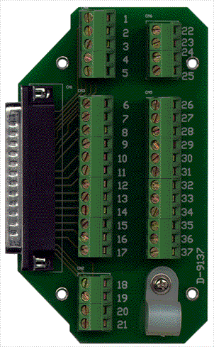
- ACLD-9137: 37-pin D-sub termination board with screw clamp terminals for easy wiring (requires ACL-10337 cable).
- DIN-37D: DIN-rail mountable termination board with 37-pin D-sub connector (requires ACL-10337 and ACL-10137 cables).
- ACLD-8125: 37-pin D-sub termination board with built-in Cold Junction Compensation (CJC) circuit for thermocouple connection (for high-gain analog input mode).
- DIN-20P: 20-pin ribbon cable termination board for compact installations.
### 6. Installation & Setup
Handling Precautions:
- The PCM-9112+ contains electrostatic-sensitive components. Handle only on a grounded anti-static mat while wearing a grounded wrist strap.
Installation Steps:
1. Unpack the module and verify all components are present.
2. Set the Rotary Switch according to the module’s position in the PC/104+ stack (see Table 1).
3. Configure Jumpers (JP1–JP5) for desired input mode, clock source, and reference voltage.
4. Connect Signal Cables to CN1 and CN2 as required.
5. Stack the Module onto the PC/104+ host board, ensuring proper alignment of connectors.
6. Secure the Stack using standoffs and screws to maintain mechanical stability.
7. Install Software Drivers and utilities from the provided CD-ROM.
Rotary Switch Configuration (Table 1):
| Rotary Position | Module Slot | CLK | IDSEL | INT | REQ | GNT |
|------------------|-------------|------|--------|------|------|------|
| 0 or 4 | Slot 1 | CLK0 | IDSEL0 | INTA | REQ0* | GNT0* |
| 1 or 5 | Slot 2 | CLK1 | IDSEL1 | INTB | REQ1* | GNT1* |
| 2 or 6 | Slot 3 | CLK2 | IDSEL2 | INTC | REQ2* | GNT2* |
| 3 or 7 | Slot 4 | CLK3 | IDSEL3 | INTD | REQ2* | GNT2* |
(*Bus Master cards only)
Jumper Settings (Table 2):
| Function | Configuration | Jumpers |
|-----------|----------------|----------|
| Analog Input Mode | Single-ended / Differential | JP1, JP4 |
| Clock Source | Internal 2 MHz / External | JP2 |
| D/A Reference Voltage | –5 V / –10 V | JP3 |
| D/A Reference Source | Internal / External | JP5 |
### 7. Performance & Capabilities
Analog Input Performance:
- 12-bit resolution ensures precise signal measurement.
- 110 kHz maximum sampling rate supports high-speed data acquisition.
- 512-word FIFO buffer minimizes data loss and CPU overhead.
Analog Output Performance:
- Dual 12-bit D/A channels provide smooth and accurate voltage output.
- Configurable output ranges (0–5 V or 0–10 V) accommodate various control applications.
Counter/Timer Performance:
- Three independent 16-bit counters allow flexible timing and counting operations.
- Internal 2 MHz clock ensures stable timing accuracy.
- External clock input option supports synchronization with external events.
Efficiency & Limitations:
- Optimized for embedded systems with limited space and power.
- No digital I/O channels (DI/DO) – replaced by expanded A/D FIFO buffer.
- Bus-mastering limitations: modules in slots 3 and 4 cannot both be bus masters due to shared REQ2/GNT2 lines.
### 8. Standards & Compliance
- Bus Standard: PC/104+ (PCI-based) compliant
- Electrical Compliance: PCI signal compatibility (excluding 64-bit extensions, JTAG, PRSNT, CLKRUN)
- Mechanical Compliance: PC/104+ stackable module form factor (96 × 90 mm)
- Safety & EMC: Designed for industrial embedded environments (meets typical CE and FCC Class A requirements)
- Software Compatibility: Compatible with ADLINK’s PCI-9112 software suite (excluding DI/DO functions)
### 9. Additional Information
Warranty:
- Standard manufacturer’s warranty (typically 1–2 years, depending on region and distributor).
Technical Support:
- ADLINK provides driver updates, software utilities, and technical documentation via its support portal.
- Application notes and example code available for integration with Windows and Linux environments.
Maintenance:
- Periodic inspection of connectors and jumpers recommended.
- Keep module free from dust and moisture.
- Handle only in ESD-safe environments.
Software & Firmware Updates:
- Compatible with ADLINK’s DAQ software utilities and SDKs.
- Firmware updates (if applicable) available through ADLINK support.
### Summary
The ADLINK PCM-9112+ is a robust, high-precision PC/104+ data acquisition module engineered for embedded and industrial applications requiring reliable analog signal measurement and generation. With 12-bit resolution, 110 kHz sampling, dual D/A outputs, and three programmable counters, it delivers versatile functionality in a compact, stackable form factor. Its configurable input modes, reference voltage options, and broad accessory support make it adaptable to a wide range of measurement and control tasks.
Designed for seamless integration into PC/104+ systems, the PCM-9112+ combines performance, flexibility, and reliability—making it an ideal choice for engineers developing embedded data acquisition, control, and automation solutions.

### 1. Product Overview
Product Name: PCM-9112+
Model: PCM-9112+
Series: PC/104+ Data Acquisition (DAQ) Module Series
Article Number: PCM-9112+
Manufacturer: ADLINK Technology Inc.
Part Number: 50-40035-200
Manual Revision: Rev. 1.03 (September 19, 2002)
The ADLINK PCM-9112+ is a compact, high-performance PC/104+ analog-to-digital (A/D) and digital-to-analog (D/A) data acquisition module designed for embedded and industrial applications. It provides 16 single-ended or 8 differential analog input channels, 12-bit resolution, and a maximum sampling rate of 110 kHz. The module also includes two 12-bit analog output channels, three independent 16-bit programmable counters, and a 512-word A/D FIFO buffer for efficient data handling.
The PCM-9112+ is mechanically and electrically compliant with the PC/104+ (PCI-based) bus standard, making it ideal for stackable embedded systems where space, reliability, and modularity are critical.
### 2. Key Features
- PC/104+ Bus Architecture: Fully compliant with the PC/104+ (PCI) specification, supporting modular stack installation and signal multiplexing for CLK, IDSEL, INT, REQ, and GNT lines.
- High-Resolution A/D Conversion: 12-bit analog-to-digital converter with up to 110 kHz sampling rate for precise signal acquisition.
- Flexible Analog Input Configuration: Supports 16 single-ended (SE) or 8 differential (DI) analog input channels, selectable via jumpers (JP1, JP4).
- Dual 12-bit D/A Outputs: Two analog output channels with configurable voltage ranges of 0–5 V or 0–10 V, depending on internal reference settings.
- Programmable Counter/Timer: Integrated 8254-compatible 3-channel, 16-bit programmable counter/timer for event counting, frequency generation, or timing control.
- Large FIFO Buffer: 512-word A/D FIFO for efficient data throughput and reduced CPU overhead.
- Configurable Reference Voltage: Internal or external D/A reference voltage selection (JP5), with internal reference options of –5 V or –10 V (JP3).
- Rotary Switch Configuration: Hardware rotary switch for assigning PCI bus signals according to module slot position in the PC/104+ stack.
- Compact Form Factor: Standard PC/104+ dimensions (96 mm × 90 mm) suitable for embedded and industrial environments.
- Software Compatibility: Compatible with the same software utilities as the PCI-9112 series (excluding DI/DO functions).
- Accessory Support: Compatible with ADLINK’s ACLD and DIN series termination and signal conditioning boards for simplified wiring and thermocouple interfacing.
### 3. Technical Specifications
Physical Characteristics:
- Form Factor: PC/104+ (PCI-based stackable module)
- Dimensions: 96 mm × 90 mm
- Weight: Approximately 100–120 g (typical for PC/104+ modules)
- Connectors:
- CN1: 20-pin analog input connector
- CN2: 20-pin analog output and counter/timer connector
- PC/104+ PCI connector
- PC/104 ISA connector (for mechanical stacking)
Analog Input (A/D):
- Channels: 16 single-ended or 8 differential (jumper-selectable)
- Resolution: 12 bits
- Sampling Rate: Up to 110 kHz
- Input Range: Configurable via software or hardware (typical ±5 V, ±10 V ranges depending on configuration)
- FIFO Buffer: 512 words
Analog Output (D/A):
- Channels: 2
- Resolution: 12 bits
- Output Range: 0–5 V or 0–10 V (selectable via internal reference voltage setting)
- Reference Voltage: Internal (–5 V or –10 V) or external (via CN2 pins 3 and 4)
Counter/Timer:
- Type: 8254-compatible programmable interval timer
- Channels: 3 independent 16-bit counters
- Clock Source: Internal 2 MHz oscillator or external clock (JP2 selectable)
- Functions: Event counting, frequency generation, pulse width measurement, and timing control
Power Requirements:
- Bus Power: Supplied through PC/104+ connector (typical +5 V DC)
- Power Consumption: Low power design suitable for embedded systems (exact current draw dependent on configuration)
Environmental:
- Operating Temperature: 0°C to +60°C (typical industrial range)
- Storage Temperature: –20°C to +80°C
- Humidity: 5% to 95% non-condensing
Materials:
- Multi-layer PCB with gold-plated edge connectors
- High-reliability components for industrial-grade operation
### 4. Functionality
The PCM-9112+ operates as a data acquisition and control interface between analog signals and a host embedded system via the PC/104+ bus.
Operation Overview:
1. Analog Input Acquisition: The onboard 12-bit A/D converter samples analog signals from up to 16 SE or 8 DI channels. The input configuration is determined by jumpers JP1 and JP4.
2. Analog Output Generation: Two 12-bit D/A converters generate analog output voltages for control or simulation tasks. Output range and reference source are configurable via JP3 and JP5.
3. Timing and Counting: The integrated 8254 timer provides three programmable counters for timing, event counting, or frequency generation.
4. Data Handling: The 512-word FIFO buffer ensures smooth data transfer to the host system, minimizing CPU load.
5. Bus Communication: The module communicates with the host CPU through the PC/104+ PCI bus, with signal routing controlled by a rotary switch to match the module’s stack position.
Applications:
- Industrial process monitoring and control
- Embedded data acquisition systems
- Laboratory instrumentation
- Signal measurement and waveform generation
- Test and automation systems
- Portable or ruggedized embedded PCs
Compatibility:
- Fully compatible with PC/104+ (PCI) embedded systems
- Software compatible with ADLINK PCI-9112 series (excluding DI/DO functions)
- Supports ADLINK’s accessory boards for extended connectivity
### 5. Components & Accessories
Included Items:
- PCM-9112+ DAQ module
- Manual and Software Utility CD-ROM
Connectors:
- CN1 (Analog Input): 20-pin header for analog input channels (AIH0–AIH7, AIL0–AIL7, AIn, A.GND, D.GND)
- CN2 (Analog Output / Counter): 20-pin header for analog outputs (AO1, AO2), external reference inputs (ExtRef1, ExtRef2), external clock (ExtCLK), external trigger (ExtTrig), gate input (GATE), counter outputs (COUT0–COUT2), and voltage reference (V.REF)
Optional Accessories:
- ACLD-9137: 37-pin D-sub termination board with screw clamp terminals for easy wiring (requires ACL-10337 cable).
- DIN-37D: DIN-rail mountable termination board with 37-pin D-sub connector (requires ACL-10337 and ACL-10137 cables).
- ACLD-8125: 37-pin D-sub termination board with built-in Cold Junction Compensation (CJC) circuit for thermocouple connection (for high-gain analog input mode).
- DIN-20P: 20-pin ribbon cable termination board for compact installations.
### 6. Installation & Setup
Handling Precautions:
- The PCM-9112+ contains electrostatic-sensitive components. Handle only on a grounded anti-static mat while wearing a grounded wrist strap.
Installation Steps:
1. Unpack the module and verify all components are present.
2. Set the Rotary Switch according to the module’s position in the PC/104+ stack (see Table 1).
3. Configure Jumpers (JP1–JP5) for desired input mode, clock source, and reference voltage.
4. Connect Signal Cables to CN1 and CN2 as required.
5. Stack the Module onto the PC/104+ host board, ensuring proper alignment of connectors.
6. Secure the Stack using standoffs and screws to maintain mechanical stability.
7. Install Software Drivers and utilities from the provided CD-ROM.
Rotary Switch Configuration (Table 1):
| Rotary Position | Module Slot | CLK | IDSEL | INT | REQ | GNT |
|------------------|-------------|------|--------|------|------|------|
| 0 or 4 | Slot 1 | CLK0 | IDSEL0 | INTA | REQ0* | GNT0* |
| 1 or 5 | Slot 2 | CLK1 | IDSEL1 | INTB | REQ1* | GNT1* |
| 2 or 6 | Slot 3 | CLK2 | IDSEL2 | INTC | REQ2* | GNT2* |
| 3 or 7 | Slot 4 | CLK3 | IDSEL3 | INTD | REQ2* | GNT2* |
(*Bus Master cards only)
Jumper Settings (Table 2):
| Function | Configuration | Jumpers |
|-----------|----------------|----------|
| Analog Input Mode | Single-ended / Differential | JP1, JP4 |
| Clock Source | Internal 2 MHz / External | JP2 |
| D/A Reference Voltage | –5 V / –10 V | JP3 |
| D/A Reference Source | Internal / External | JP5 |
### 7. Performance & Capabilities
Analog Input Performance:
- 12-bit resolution ensures precise signal measurement.
- 110 kHz maximum sampling rate supports high-speed data acquisition.
- 512-word FIFO buffer minimizes data loss and CPU overhead.
Analog Output Performance:
- Dual 12-bit D/A channels provide smooth and accurate voltage output.
- Configurable output ranges (0–5 V or 0–10 V) accommodate various control applications.
Counter/Timer Performance:
- Three independent 16-bit counters allow flexible timing and counting operations.
- Internal 2 MHz clock ensures stable timing accuracy.
- External clock input option supports synchronization with external events.
Efficiency & Limitations:
- Optimized for embedded systems with limited space and power.
- No digital I/O channels (DI/DO) – replaced by expanded A/D FIFO buffer.
- Bus-mastering limitations: modules in slots 3 and 4 cannot both be bus masters due to shared REQ2/GNT2 lines.
### 8. Standards & Compliance
- Bus Standard: PC/104+ (PCI-based) compliant
- Electrical Compliance: PCI signal compatibility (excluding 64-bit extensions, JTAG, PRSNT, CLKRUN)
- Mechanical Compliance: PC/104+ stackable module form factor (96 × 90 mm)
- Safety & EMC: Designed for industrial embedded environments (meets typical CE and FCC Class A requirements)
- Software Compatibility: Compatible with ADLINK’s PCI-9112 software suite (excluding DI/DO functions)
### 9. Additional Information
Warranty:
- Standard manufacturer’s warranty (typically 1–2 years, depending on region and distributor).
Technical Support:
- ADLINK provides driver updates, software utilities, and technical documentation via its support portal.
- Application notes and example code available for integration with Windows and Linux environments.
Maintenance:
- Periodic inspection of connectors and jumpers recommended.
- Keep module free from dust and moisture.
- Handle only in ESD-safe environments.
Software & Firmware Updates:
- Compatible with ADLINK’s DAQ software utilities and SDKs.
- Firmware updates (if applicable) available through ADLINK support.
### Summary
The ADLINK PCM-9112+ is a robust, high-precision PC/104+ data acquisition module engineered for embedded and industrial applications requiring reliable analog signal measurement and generation. With 12-bit resolution, 110 kHz sampling, dual D/A outputs, and three programmable counters, it delivers versatile functionality in a compact, stackable form factor. Its configurable input modes, reference voltage options, and broad accessory support make it adaptable to a wide range of measurement and control tasks.
Designed for seamless integration into PC/104+ systems, the PCM-9112+ combines performance, flexibility, and reliability—making it an ideal choice for engineers developing embedded data acquisition, control, and automation solutions.

-
PCM-9112_50-40035-200.pdf
Manual
- EBC-1200 - Embedded 3,5'' board VGA LAN PC104+
- ACL-10337 - 2*20 pin to DB 37 slot adapter
- DIN-37D-01 - 37pin D-type panel DIN rail w/o cable
- DIN-20P-01 - 20pin header termination board DIN rail
- ACLD-9137-01 - Direct 37 small screw terminal
- ACLD-9138-01 - Panel general purpose, 2*20 small screw terminal
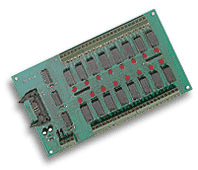
- ACLD-9185-01 - isolated 16 DO Relay panel
- ACLD-9188 - Panel for mounting low pass filter etc.
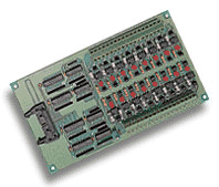
- ACLD-9182A-01 - isolated 16 DI (DC) panel