DIN-68S-01
SUCHEN SIE DIE PASSENDE
INDUSTRIELLE LÖSUNG?
Entdecken Sie Embedded-, Kommunikations- und Automatisierungslösungen für Ihre Anwendung.
- Simultaneous 4-Channel Analog Input:
Four differential analog input channels with simultaneous sampling capability, ensuring phase-coherent data acquisition across all channels.
- High Resolution and Speed:
16-bit resolution with a maximum sampling rate of 800 kS/s per channel.
- Programmable Input Ranges:
Bipolar ranges: ±10V, ±5V, ±2.5V, ±1.25V
Unipolar ranges: 0–10V, 0–5V, 0–2.5V, 0–1.25V
- Auto-Calibration:
Fully automatic calibration for both A/D and D/A circuits, ensuring long-term accuracy and stability.
- Dual 12-bit Analog Outputs:
Two analog output channels with 1 MS/s update rate, ±10V or 0–10V output range, and 1k-sample FIFO per channel.
- Digital I/O:
24 programmable TTL/CMOS-compatible digital I/O lines (8255A compatible).
- Counters/Timers:
Two 16-bit general-purpose up/down counters with programmable clock and gate sources.
- Triggering Flexibility:
Supports software, external analog, external digital, and SSI (System Synchronization Interface) triggers.
Four trigger modes: post-trigger, pre-trigger, delay-trigger, and middle-trigger.
- Bus-Mastering DMA:
High-speed data transfer via PCI bus-mastering DMA with scatter/gather capability for efficient memory usage.
- System Synchronization Interface (SSI):
Enables synchronization of multiple PXI cards for multi-channel, multi-board data acquisition.
- Software Configurable:
Completely jumper-less design with full software configuration for gain, range, and trigger settings.
- Software Support:
Includes drivers and libraries for Windows and Linux, LabVIEW® PnP VIs, and ActiveX controls.
Four differential analog input channels with simultaneous sampling capability, ensuring phase-coherent data acquisition across all channels.
- High Resolution and Speed:
16-bit resolution with a maximum sampling rate of 800 kS/s per channel.
- Programmable Input Ranges:
Bipolar ranges: ±10V, ±5V, ±2.5V, ±1.25V
Unipolar ranges: 0–10V, 0–5V, 0–2.5V, 0–1.25V
- Auto-Calibration:
Fully automatic calibration for both A/D and D/A circuits, ensuring long-term accuracy and stability.
- Dual 12-bit Analog Outputs:
Two analog output channels with 1 MS/s update rate, ±10V or 0–10V output range, and 1k-sample FIFO per channel.
- Digital I/O:
24 programmable TTL/CMOS-compatible digital I/O lines (8255A compatible).
- Counters/Timers:
Two 16-bit general-purpose up/down counters with programmable clock and gate sources.
- Triggering Flexibility:
Supports software, external analog, external digital, and SSI (System Synchronization Interface) triggers.
Four trigger modes: post-trigger, pre-trigger, delay-trigger, and middle-trigger.
- Bus-Mastering DMA:
High-speed data transfer via PCI bus-mastering DMA with scatter/gather capability for efficient memory usage.
- System Synchronization Interface (SSI):
Enables synchronization of multiple PXI cards for multi-channel, multi-board data acquisition.
- Software Configurable:
Completely jumper-less design with full software configuration for gain, range, and trigger settings.
- Software Support:
Includes drivers and libraries for Windows and Linux, LabVIEW® PnP VIs, and ActiveX controls.
Comprehensive Product Summary – ADLINK PXI-2016 Multi-Function Data Acquisition Card
### 1. Product Overview
Product Name: PXI-2016
Model: PXI-2016
Series: DAQ/PXI-20XX Series
Article Number: PXI-2016
Manufacturer: ADLINK Technology Inc.
Part Number: 50-11020-1030
Manual Revision: 2.00 (April 20, 2006)
Product Type: PXI Bus Multi-Function Data Acquisition (DAQ) Card
Form Factor: PXI (CompactPCI) standard form factor
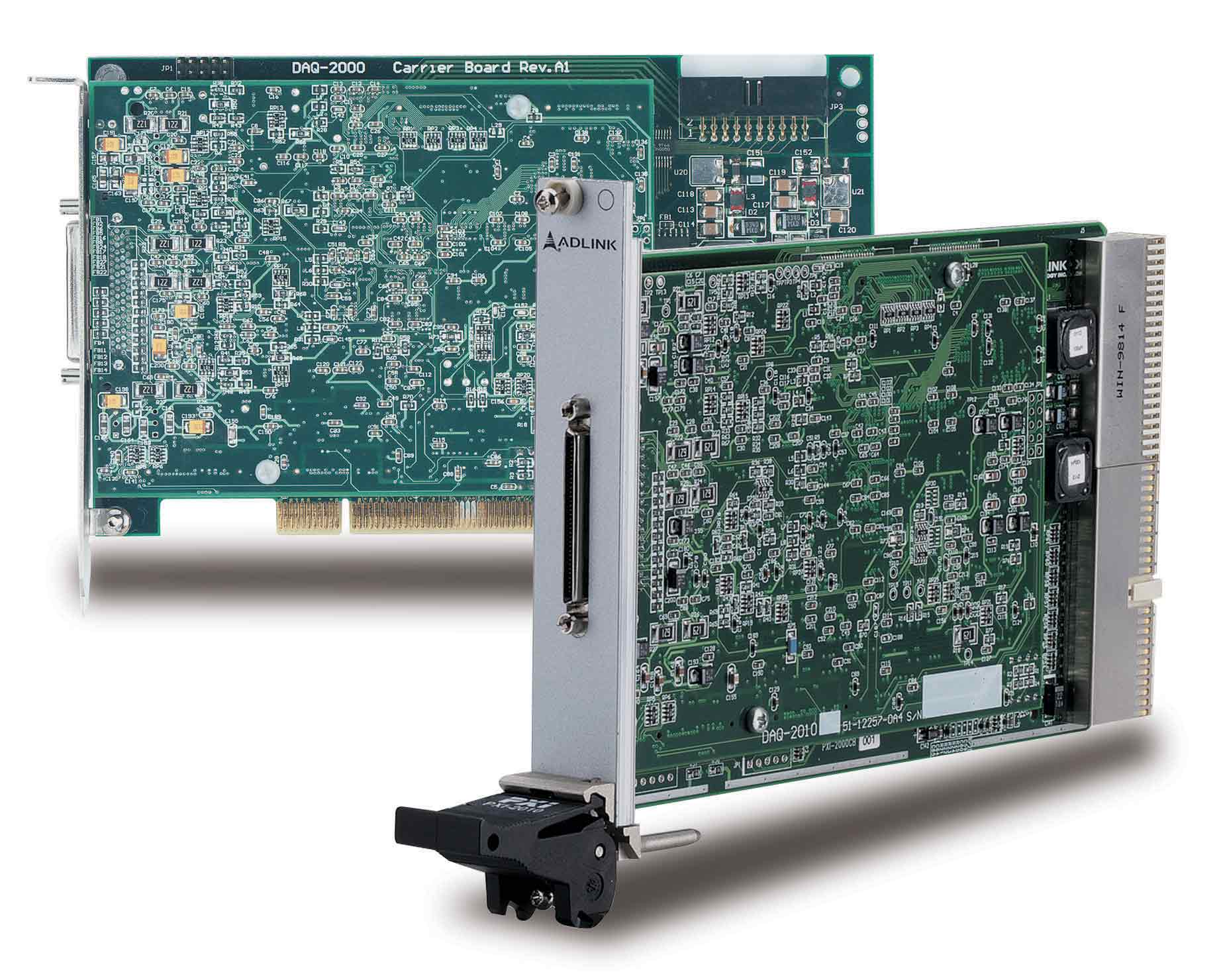
The ADLINK PXI-2016 is a high-performance, 4-channel, simultaneous-sampling, 16-bit analog-to-digital (A/D) data acquisition card designed for PXI systems. It provides a maximum sampling rate of 800 kS/s per channel and integrates analog input, analog output, digital I/O, and counter/timer functions in a single module. The PXI-2016 is part of ADLINK’s DAQ/PXI-20XX series, which includes models 2010, 2005, 2006, and 2016, each optimized for different sampling rates and resolutions.
### 2. Key Features
- Simultaneous 4-Channel Analog Input:
Four differential analog input channels with simultaneous sampling capability, ensuring phase-coherent data acquisition across all channels.
- High Resolution and Speed:
16-bit resolution with a maximum sampling rate of 800 kS/s per channel.
- Programmable Input Ranges:
Bipolar ranges: ±10V, ±5V, ±2.5V, ±1.25V
Unipolar ranges: 0–10V, 0–5V, 0–2.5V, 0–1.25V
- Auto-Calibration:
Fully automatic calibration for both A/D and D/A circuits, ensuring long-term accuracy and stability.
- Dual 12-bit Analog Outputs:
Two analog output channels with 1 MS/s update rate, ±10V or 0–10V output range, and 1k-sample FIFO per channel.
- Digital I/O:
24 programmable TTL/CMOS-compatible digital I/O lines (8255A compatible).
- Counters/Timers:
Two 16-bit general-purpose up/down counters with programmable clock and gate sources.
- Triggering Flexibility:
Supports software, external analog, external digital, and SSI (System Synchronization Interface) triggers.
Four trigger modes: post-trigger, pre-trigger, delay-trigger, and middle-trigger.
- Bus-Mastering DMA:
High-speed data transfer via PCI bus-mastering DMA with scatter/gather capability for efficient memory usage.
- System Synchronization Interface (SSI):
Enables synchronization of multiple PXI cards for multi-channel, multi-board data acquisition.
- Software Configurable:
Completely jumper-less design with full software configuration for gain, range, and trigger settings.
- Software Support:
Includes drivers and libraries for Windows and Linux, LabVIEW® PnP VIs, and ActiveX controls.
### 3. Technical Specifications
Analog Input (AI):
- Channels: 4 differential, simultaneous sampling
- Resolution: 16 bits, no missing codes
- Sampling Rate: Up to 800 kS/s per channel
- Input Range: ±10V, ±5V, ±2.5V, ±1.25V or 0–10V, 0–5V, 0–2.5V, 0–1.25V
- Input Impedance: 1 GΩ / 100 pF
- Common Mode Voltage Range: ±11V
- Overvoltage Protection: ±30V (power on), ±15V (power off)
- Input Coupling: DC
- FIFO Buffer: 512 samples total
- Bandwidth (-3 dB): up to 840 kHz (±10V range)
- Large Signal Bandwidth (1% THD): 300 kHz
- System Noise: 1.6–3.4 LSB rms depending on range
- CMRR (DC–60 Hz): up to 95 dB
- Offset Error: ±60 mV max (before calibration), ±1 mV max (after calibration)
- Gain Error: ±0.6% (before calibration), ±0.03% (after calibration)
Analog Output (AO):
- Channels: 2
- Resolution: 12 bits
- Update Rate: 1 MS/s
- Output Range: ±10V or 0–10V (internal reference), ±AOEXTREF (external reference)
- FIFO Buffer: 1k samples per channel (2k when one channel active)
- Settling Time: 3 µs to 0.5 LSB
- Slew Rate: 20 V/µs
- Output Impedance: 0.3 Ω typical
- Output Drive: ±5 mA max
- Protection: Short-circuit to ground
- Power-on State: 0V steady-state
- Relative Accuracy: ±0.5 LSB typical
- DNL: ±0.5 LSB typical
- Offset Error: ±80 mV max (before calibration), ±1 mV max (after calibration)
- Gain Error: ±0.8% (before calibration), ±0.02% (after calibration)
Digital I/O:
- Channels: 24 programmable I/O lines (8255A compatible)
- Logic Levels: TTL/CMOS
- Input Low: ≤0.8V, Output Low: ≤0.5V @ 8 mA
- Input High: ≥2.0V, Output High: ≥2.7V @ 400 µA
Counters/Timers:
- Channels: 2 independent 16-bit up/down counters
- Clock Source: Internal or external (up to 10 MHz)
- Modes: 8 programmable modes (event counting, pulse generation, period/pulse-width measurement, etc.)
- Compatibility: TTL
Triggering:
- Sources: Software, external analog, external digital, SSI
- Analog Trigger: ±Full-scale internal, ±10V external, 8-bit resolution, programmable hysteresis
- Digital Trigger: TTL/CMOS compatible, 10 ns minimum pulse width
- Bandwidth: 400 kHz
Clocking:
- Internal Clock: 40 MHz
- External Clock Input: 1–40 MHz, TTL-compatible
Physical Characteristics:
- Dimensions: 100 mm × 160 mm (PXI standard)
- Connector: 68-pin VHDCI (AMP-787254-1 or equivalent)
- Power Consumption: +5VDC @ 2.52 A (typical)
- Weight: Approx. 250 g
Environmental:
- Operating Temperature: 0°C to 55°C
- Storage Temperature: -20°C to 80°C
- Humidity: 10–90% RH (operating), 5–95% RH (storage), non-condensing
### 4. Functionality
The PXI-2016 performs high-speed, simultaneous analog-to-digital conversion across four channels, enabling precise time-aligned sampling for transient or multi-sensor measurements. The onboard 40 MHz clock or an external clock source drives the timing engine. Data acquisition can be triggered by software, external analog/digital signals, or synchronized via SSI.
Use Cases:
- Automotive and cable testing
- Transient signal capture and waveform analysis
- Automated Test Equipment (ATE)
- Laboratory and process automation
- Biotech and medical instrumentation
Compatibility:
- PXI and CompactPCI chassis
- Windows 98/NT/2000/XP and Linux
- LabVIEW®, Visual Basic, C/C++, Delphi, and ActiveX environments
### 5. Components & Accessories
Included Items:
- PXI-2016 DAQ card
- ADLINK All-in-One Software CD
- Software Installation Guide
- User’s Manual
Connectors:
- 68-pin VHDCI connector for analog, digital, and timing I/O
- PXI backplane connector for power and synchronization
- Optional SSI (System Synchronization Interface) via PXI backplane
Optional Accessories:
- ACL-SSI synchronization cable (for multi-card synchronization)
- Shielded VHDCI cable assemblies
- Terminal boards for signal breakout
### 6. Installation & Setup
Requirements:
- PXI or CompactPCI chassis with available slot
- +5VDC power supply (2.52 A typical)
- Compatible operating system and driver software
Installation Steps:
1. Power off the PXI chassis.
2. Insert the PXI-2016 into an available slot.
3. Secure the module and power on the system.
4. Install ADLINK drivers from the provided CD.
5. Use the PCI_SCAN utility to verify system configuration.
Configuration:
- Fully plug-and-play; no jumpers required.
- Software-configurable base address, DMA, and IRQ.
- Automatic resource allocation by BIOS and driver.
### 7. Performance & Capabilities
- A/D Conversion: 16-bit resolution, 800 kS/s simultaneous sampling
- D/A Conversion: 12-bit resolution, 1 MS/s update rate
- DMA Transfer: Bus-mastering DMA with scatter/gather for high throughput
- FIFO Buffers: 512-sample A/D FIFO, 1k-sample D/A FIFO per channel
- Trigger Modes: Pre-, post-, delay-, and middle-trigger with re-trigger capability
- Synchronization: SSI/PXI trigger bus for multi-card timing alignment
- Accuracy: Post-calibration gain error ≤0.03%, offset error ≤1 mV
- Noise Performance: ≤3.4 LSB rms typical
- Bandwidth: Up to 840 kHz (-3 dB) small-signal bandwidth
Limitations:
- Maximum external clock frequency: 40 MHz
- Analog trigger bandwidth limited to 400 kHz
- Output drive current limited to ±5 mA
### 8. Standards & Compliance
- Bus Interface: PXI (CompactPCI) compliant
- Electrical Compatibility: TTL/CMOS logic levels
- Safety & EMC: Designed to meet industrial EMC and safety standards
- Software Standards: Compatible with NI LabVIEW®, ActiveX, and standard Windows/Linux APIs
- Environmental Compliance: RoHS-compliant manufacturing (depending on production date)
### 9. Additional Information
Calibration:
- Factory-calibrated with stored constants in onboard EEPROM
- Auto-calibration feature using internal 5.000V reference (±2 ppm/°C)
- Long-term stability: 6 ppm/1000 hours
- Three user-modifiable calibration banks for different environments
Maintenance:
- Recommended warm-up time: 15 minutes before calibration
- Periodic recalibration advised for optimal accuracy
Warranty:
- Standard 2-year limited warranty (1 year in China)
- Covers manufacturing defects and hardware failures under normal use
- Excludes damage from misuse, environmental factors, or unauthorized repair
Technical Support:
- Website: [www.adlinktech.com](http://www.adlinktech.com)
- Email: service@adlinktech.com
- Phone: +886-2-82265877
- Fax: +886-2-82265717
- Address: 9F, No. 166, Jian Yi Road, Chungho City, Taipei 235, Taiwan
Software Support:
- D2K-DASK: Windows driver and DLL library
- D2K-DASK/X: Linux shared library
- DAQ-LVIEW PnP: LabVIEW® driver package
- D2K-OCX: ActiveX control library
- DAQBench: Optional ActiveX-based GUI toolkit
Updates & Documentation:
- Software and firmware updates available via ADLINK website
- User manuals, programming references, and sample code included on CD
### Summary
The ADLINK PXI-2016 is a robust, high-precision, multi-function PXI data acquisition card engineered for demanding measurement and automation applications. With 16-bit, 800 kS/s simultaneous sampling, dual 12-bit analog outputs, 24 digital I/O lines, and dual 16-bit counters, it provides a complete, synchronized data acquisition and generation solution. Its flexible triggering, auto-calibration, and software configurability make it ideal for laboratory, industrial, and research environments requiring reliable, high-speed, and accurate data capture.

### 1. Product Overview
Product Name: PXI-2016
Model: PXI-2016
Series: DAQ/PXI-20XX Series
Article Number: PXI-2016
Manufacturer: ADLINK Technology Inc.
Part Number: 50-11020-1030
Manual Revision: 2.00 (April 20, 2006)
Product Type: PXI Bus Multi-Function Data Acquisition (DAQ) Card
Form Factor: PXI (CompactPCI) standard form factor
The ADLINK PXI-2016 is a high-performance, 4-channel, simultaneous-sampling, 16-bit analog-to-digital (A/D) data acquisition card designed for PXI systems. It provides a maximum sampling rate of 800 kS/s per channel and integrates analog input, analog output, digital I/O, and counter/timer functions in a single module. The PXI-2016 is part of ADLINK’s DAQ/PXI-20XX series, which includes models 2010, 2005, 2006, and 2016, each optimized for different sampling rates and resolutions.
### 2. Key Features
- Simultaneous 4-Channel Analog Input:
Four differential analog input channels with simultaneous sampling capability, ensuring phase-coherent data acquisition across all channels.
- High Resolution and Speed:
16-bit resolution with a maximum sampling rate of 800 kS/s per channel.
- Programmable Input Ranges:
Bipolar ranges: ±10V, ±5V, ±2.5V, ±1.25V
Unipolar ranges: 0–10V, 0–5V, 0–2.5V, 0–1.25V
- Auto-Calibration:
Fully automatic calibration for both A/D and D/A circuits, ensuring long-term accuracy and stability.
- Dual 12-bit Analog Outputs:
Two analog output channels with 1 MS/s update rate, ±10V or 0–10V output range, and 1k-sample FIFO per channel.
- Digital I/O:
24 programmable TTL/CMOS-compatible digital I/O lines (8255A compatible).
- Counters/Timers:
Two 16-bit general-purpose up/down counters with programmable clock and gate sources.
- Triggering Flexibility:
Supports software, external analog, external digital, and SSI (System Synchronization Interface) triggers.
Four trigger modes: post-trigger, pre-trigger, delay-trigger, and middle-trigger.
- Bus-Mastering DMA:
High-speed data transfer via PCI bus-mastering DMA with scatter/gather capability for efficient memory usage.
- System Synchronization Interface (SSI):
Enables synchronization of multiple PXI cards for multi-channel, multi-board data acquisition.
- Software Configurable:
Completely jumper-less design with full software configuration for gain, range, and trigger settings.
- Software Support:
Includes drivers and libraries for Windows and Linux, LabVIEW® PnP VIs, and ActiveX controls.
### 3. Technical Specifications
Analog Input (AI):
- Channels: 4 differential, simultaneous sampling
- Resolution: 16 bits, no missing codes
- Sampling Rate: Up to 800 kS/s per channel
- Input Range: ±10V, ±5V, ±2.5V, ±1.25V or 0–10V, 0–5V, 0–2.5V, 0–1.25V
- Input Impedance: 1 GΩ / 100 pF
- Common Mode Voltage Range: ±11V
- Overvoltage Protection: ±30V (power on), ±15V (power off)
- Input Coupling: DC
- FIFO Buffer: 512 samples total
- Bandwidth (-3 dB): up to 840 kHz (±10V range)
- Large Signal Bandwidth (1% THD): 300 kHz
- System Noise: 1.6–3.4 LSB rms depending on range
- CMRR (DC–60 Hz): up to 95 dB
- Offset Error: ±60 mV max (before calibration), ±1 mV max (after calibration)
- Gain Error: ±0.6% (before calibration), ±0.03% (after calibration)
Analog Output (AO):
- Channels: 2
- Resolution: 12 bits
- Update Rate: 1 MS/s
- Output Range: ±10V or 0–10V (internal reference), ±AOEXTREF (external reference)
- FIFO Buffer: 1k samples per channel (2k when one channel active)
- Settling Time: 3 µs to 0.5 LSB
- Slew Rate: 20 V/µs
- Output Impedance: 0.3 Ω typical
- Output Drive: ±5 mA max
- Protection: Short-circuit to ground
- Power-on State: 0V steady-state
- Relative Accuracy: ±0.5 LSB typical
- DNL: ±0.5 LSB typical
- Offset Error: ±80 mV max (before calibration), ±1 mV max (after calibration)
- Gain Error: ±0.8% (before calibration), ±0.02% (after calibration)
Digital I/O:
- Channels: 24 programmable I/O lines (8255A compatible)
- Logic Levels: TTL/CMOS
- Input Low: ≤0.8V, Output Low: ≤0.5V @ 8 mA
- Input High: ≥2.0V, Output High: ≥2.7V @ 400 µA
Counters/Timers:
- Channels: 2 independent 16-bit up/down counters
- Clock Source: Internal or external (up to 10 MHz)
- Modes: 8 programmable modes (event counting, pulse generation, period/pulse-width measurement, etc.)
- Compatibility: TTL
Triggering:
- Sources: Software, external analog, external digital, SSI
- Analog Trigger: ±Full-scale internal, ±10V external, 8-bit resolution, programmable hysteresis
- Digital Trigger: TTL/CMOS compatible, 10 ns minimum pulse width
- Bandwidth: 400 kHz
Clocking:
- Internal Clock: 40 MHz
- External Clock Input: 1–40 MHz, TTL-compatible
Physical Characteristics:
- Dimensions: 100 mm × 160 mm (PXI standard)
- Connector: 68-pin VHDCI (AMP-787254-1 or equivalent)
- Power Consumption: +5VDC @ 2.52 A (typical)
- Weight: Approx. 250 g
Environmental:
- Operating Temperature: 0°C to 55°C
- Storage Temperature: -20°C to 80°C
- Humidity: 10–90% RH (operating), 5–95% RH (storage), non-condensing
### 4. Functionality
The PXI-2016 performs high-speed, simultaneous analog-to-digital conversion across four channels, enabling precise time-aligned sampling for transient or multi-sensor measurements. The onboard 40 MHz clock or an external clock source drives the timing engine. Data acquisition can be triggered by software, external analog/digital signals, or synchronized via SSI.
Use Cases:
- Automotive and cable testing
- Transient signal capture and waveform analysis
- Automated Test Equipment (ATE)
- Laboratory and process automation
- Biotech and medical instrumentation
Compatibility:
- PXI and CompactPCI chassis
- Windows 98/NT/2000/XP and Linux
- LabVIEW®, Visual Basic, C/C++, Delphi, and ActiveX environments
### 5. Components & Accessories
Included Items:
- PXI-2016 DAQ card
- ADLINK All-in-One Software CD
- Software Installation Guide
- User’s Manual
Connectors:
- 68-pin VHDCI connector for analog, digital, and timing I/O
- PXI backplane connector for power and synchronization
- Optional SSI (System Synchronization Interface) via PXI backplane
Optional Accessories:
- ACL-SSI synchronization cable (for multi-card synchronization)
- Shielded VHDCI cable assemblies
- Terminal boards for signal breakout
### 6. Installation & Setup
Requirements:
- PXI or CompactPCI chassis with available slot
- +5VDC power supply (2.52 A typical)
- Compatible operating system and driver software
Installation Steps:
1. Power off the PXI chassis.
2. Insert the PXI-2016 into an available slot.
3. Secure the module and power on the system.
4. Install ADLINK drivers from the provided CD.
5. Use the PCI_SCAN utility to verify system configuration.
Configuration:
- Fully plug-and-play; no jumpers required.
- Software-configurable base address, DMA, and IRQ.
- Automatic resource allocation by BIOS and driver.
### 7. Performance & Capabilities
- A/D Conversion: 16-bit resolution, 800 kS/s simultaneous sampling
- D/A Conversion: 12-bit resolution, 1 MS/s update rate
- DMA Transfer: Bus-mastering DMA with scatter/gather for high throughput
- FIFO Buffers: 512-sample A/D FIFO, 1k-sample D/A FIFO per channel
- Trigger Modes: Pre-, post-, delay-, and middle-trigger with re-trigger capability
- Synchronization: SSI/PXI trigger bus for multi-card timing alignment
- Accuracy: Post-calibration gain error ≤0.03%, offset error ≤1 mV
- Noise Performance: ≤3.4 LSB rms typical
- Bandwidth: Up to 840 kHz (-3 dB) small-signal bandwidth
Limitations:
- Maximum external clock frequency: 40 MHz
- Analog trigger bandwidth limited to 400 kHz
- Output drive current limited to ±5 mA
### 8. Standards & Compliance
- Bus Interface: PXI (CompactPCI) compliant
- Electrical Compatibility: TTL/CMOS logic levels
- Safety & EMC: Designed to meet industrial EMC and safety standards
- Software Standards: Compatible with NI LabVIEW®, ActiveX, and standard Windows/Linux APIs
- Environmental Compliance: RoHS-compliant manufacturing (depending on production date)
### 9. Additional Information
Calibration:
- Factory-calibrated with stored constants in onboard EEPROM
- Auto-calibration feature using internal 5.000V reference (±2 ppm/°C)
- Long-term stability: 6 ppm/1000 hours
- Three user-modifiable calibration banks for different environments
Maintenance:
- Recommended warm-up time: 15 minutes before calibration
- Periodic recalibration advised for optimal accuracy
Warranty:
- Standard 2-year limited warranty (1 year in China)
- Covers manufacturing defects and hardware failures under normal use
- Excludes damage from misuse, environmental factors, or unauthorized repair
Technical Support:
- Website: [www.adlinktech.com](http://www.adlinktech.com)
- Email: service@adlinktech.com
- Phone: +886-2-82265877
- Fax: +886-2-82265717
- Address: 9F, No. 166, Jian Yi Road, Chungho City, Taipei 235, Taiwan
Software Support:
- D2K-DASK: Windows driver and DLL library
- D2K-DASK/X: Linux shared library
- DAQ-LVIEW PnP: LabVIEW® driver package
- D2K-OCX: ActiveX control library
- DAQBench: Optional ActiveX-based GUI toolkit
Updates & Documentation:
- Software and firmware updates available via ADLINK website
- User manuals, programming references, and sample code included on CD
### Summary
The ADLINK PXI-2016 is a robust, high-precision, multi-function PXI data acquisition card engineered for demanding measurement and automation applications. With 16-bit, 800 kS/s simultaneous sampling, dual 12-bit analog outputs, 24 digital I/O lines, and dual 16-bit counters, it provides a complete, synchronized data acquisition and generation solution. Its flexible triggering, auto-calibration, and software configurability make it ideal for laboratory, industrial, and research environments requiring reliable, high-speed, and accurate data capture.
-
DAQ-2000Series_Manual_5.pdf
Manual
-
PXI-2000Series_Manual_4.pdf
Manual
- DIN-68S-01 - 68pin SCSI-II termination board DIN rail w/o cable
- ACL-10568-1 - SCSI-VHDCI cable 1m for DAQ series
- ACL-10568-2 - SCSI-VHDCI cable 2m for DAQ series
- ACL-10568-3 - SCSI-VHDCI cable 3m for DAQ series