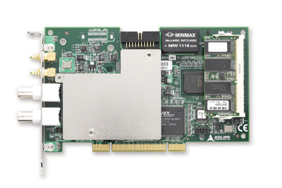
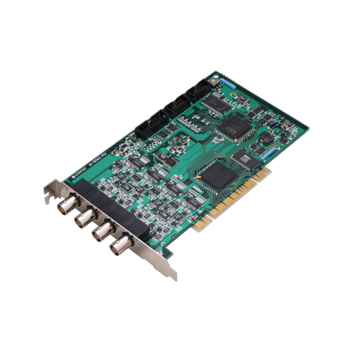
Comprehensive Product Summary – ADLINK PCI‑9810
### 1. Product Overview
Product Name: PCI‑9810
Model: PCI‑9810
Series: NuDAQ PCI‑9812/9812A/9810 Series
Article Number: PCI‑9810
Manufacturer: ADLINK Technology Inc. (Taipei, Taiwan, R.O.C.)
Product Type: 4‑Channel, 10‑bit, 20 MS/s Simultaneous‑Sampling Analog Input PCI Data Acquisition Card
The ADLINK PCI‑9810 is a high‑speed, 32‑bit PCI‑bus analog‑to‑digital (A/D) acquisition card designed for simultaneous sampling of up to four analog channels at rates up to 20 MS/s per channel. It belongs to ADLINK’s NuDAQ PCI‑9812/9812A/9810 family, which includes 10‑bit and 12‑bit variants. The PCI‑9810 specifically provides 10‑bit resolution and a 32 k‑sample FIFO buffer for high‑speed, continuous data capture in industrial, scientific, and engineering applications.
### 2. Key Features
- High‑Speed Simultaneous Sampling:
Four single‑ended analog input channels, each capable of 20 MS/s simultaneous sampling using dedicated A/D converters (Burr‑Brown ADS800 series).
- Resolution:
10‑bit analog‑to‑digital conversion accuracy.
- Input Range and Impedance:
Bipolar input ranges of ±1 V or ±5 V, selectable via solder jumpers. Input impedance options include 50 Ω, 1.25 kΩ, or 15 MΩ, allowing adaptation to various signal sources.
- FIFO Buffer:
On‑board 32 k‑sample (32 k‑word) A/D FIFO memory for temporary data buffering, preventing data loss during high‑speed acquisition.
- Triggering Flexibility:
Supports software, analog threshold, and external digital triggers. Trigger modes include software, pre‑trigger, post‑trigger, middle‑trigger, and delay‑trigger.
- Clock Sources:
Internal 40 MHz time base or external clock input (sine wave or digital). External clock frequency range: 20 kHz–40 MHz.
- Bus Mastering DMA:
Direct memory access (DMA) data transfer for high‑speed throughput without CPU intervention.
- Connectors:
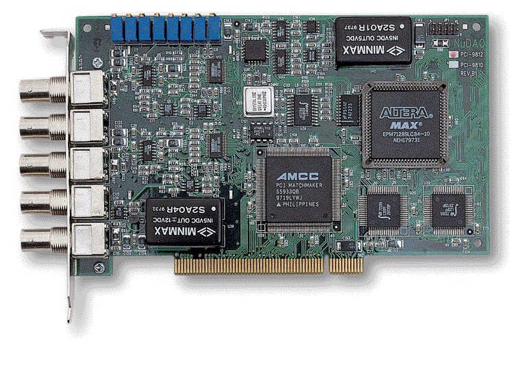
Five BNC connectors (four analog inputs + one external sine clock) and one 10‑pin ribbon header for digital I/O and external digital clock/trigger.
- Plug‑and‑Play PCI Interface:
Fully compliant with 32‑bit PCI bus architecture, automatic resource allocation (IRQ and I/O address).
- Software Support:
Compatible with ADLINK’s PCIS‑DASK driver library, DAQBench ActiveX controls, LabVIEW VIs, and DASYLab software for data acquisition and analysis.
- Applications:
Ideal for vibration analysis, ultrasonic measurement, image digitizing, biomedical instrumentation, automated test equipment (ATE), and high‑speed signal digitization.
### 3. Technical Specifications
Analog Input:
- Channels: 4 single‑ended
- Resolution: 10 bits
- Sampling Rate: Up to 20 MS/s per channel
- Input Ranges: ±1 V or ±5 V (bipolar)
- Input Impedance (solder‑selectable):
- 50 Ω (±1 V or ±5 V)
- 1.25 kΩ (±5 V only)
- 15 MΩ (±1 V only)
- Accuracy: ±1.5 % typical at 25 °C
- DNL: ±0.4 LSB typical, ±1.0 LSB max
- INL: ±1.9 LSB typical
- Input Coupling: DC
- Overvoltage Protection: ±10 V typical
External Clock Inputs:
- Sine Wave Clock (BNC J5):
- Coupling: AC
- Impedance: 50 Ω
- Frequency: 300 kHz–40 MHz
- Input Range: 1.0–2.0 Vpp
- Overvoltage Protection: 2.5 Vpp
- Digital Clock (JP1 Pin 1):
- Coupling: DC
- Impedance: 50 Ω
- Compatibility: 5 V TTL
- Frequency: 20 kHz–40 MHz
- Overvoltage Protection: Diode clamping (−0.3 V to +5.3 V)
Digital Inputs:
- Channels: 3 TTL‑compatible inputs (JP1 Pins 5, 7, 9)
- Pull‑down Resistors: 10 kΩ
- Logic Levels:
- Low: 0–0.8 V
- High: 2.0–5.5 V
- Overvoltage Protection: Diode clamping (−0.3 V to +5.3 V)
Triggering:
- Sources: Software, analog (CH0–CH3), external digital (TTL)
- Modes: Software, pre‑trigger, post‑trigger, middle‑trigger, delay‑trigger
- Analog Trigger Sensitivity: 256 steps across full‑scale range
- Digital Trigger: Rising/falling edge, 25 ns minimum pulse width
FIFO Buffer:
- Capacity: 32 k samples (PCI‑9810)
- Data Transfer: Bus‑mastering DMA
Physical and Environmental:
- Dimensions: 173 mm (L) × 108 mm (H) (excluding connectors)
- Weight: Approx. 200 g
- Operating Temperature: 0 °C – 40 °C
- Storage Temperature: −20 °C – 70 °C
- Humidity: 5 – 95 % RH, non‑condensing
- Power Requirement: +5 V @ 1 A typical
I/O Connectors:
- 5 × BNC (CH0–CH3, Ext. Sine CLK)
- 1 × 10‑pin ribbon header (JP1: Ext. Digital CLK, TRIG, DI0–DI2, GND)
### 4. Functionality
The PCI‑9810 performs high‑speed analog‑to‑digital conversion across four simultaneous channels. Each channel uses a dedicated 10‑bit ADC, enabling true simultaneous sampling without multiplexing delays. The card’s internal 40 MHz clock or external clock source defines the sampling rate. Data is temporarily stored in the on‑board 32 k‑sample FIFO before being transferred to host memory via bus‑mastering DMA.
Use Cases and Applications:
- Vibration and Acoustic Testing: Captures high‑frequency mechanical or acoustic signals.
- Ultrasonic and Biomedical Measurement: Digitizes ultrasonic echo or bio‑signal waveforms.
- Image and Video Digitization: Converts analog video or CCD sensor outputs into digital data streams.
- ATE and Scientific Research: Provides precise, synchronized data acquisition for laboratory and industrial automation systems.
- RF/Baseband Digitization: Suitable for intermediate‑frequency (IF) and baseband signal capture.
Compatibility:
- PCI 2.1 compliant, 32‑bit, 33 MHz bus interface.
- Supported OS: DOS, Windows 95/98/NT (via PCIS‑DASK drivers).
- Software integration with LabVIEW, DASYLab, and ADLINK DAQBench ActiveX.
### 5. Components & Accessories
Included Items:
- PCI‑9810 data acquisition card
- Five BNC terminators
- ADLINK “All‑in‑One” software CD (drivers, utilities, libraries)
- User’s Guide and installation documentation
Connectors and Pin Assignments:
- BNC J1–J4: Analog input channels 0–3
- BNC J5: External sine wave clock input
- JP1 (10‑pin header):
- Pin 1: External Digital Clock
- Pin 3: External Digital Trigger
- Pins 5, 7, 9: Digital Inputs 0–2
- Even pins: Ground
Optional Accessories:
- Shielded BNC cables
- External clock signal generators
- Termination boards or breakout cables for JP1 digital I/O
### 6. Installation & Setup
Hardware Installation:
1. Power off the PC and remove the cover.
2. Insert the PCI‑9810 into an available 32‑bit PCI slot (do not use ISA slots).
3. Secure the bracket and reconnect system power.
4. The card is plug‑and‑play; BIOS automatically assigns IRQ and I/O addresses.
Software Installation (Windows 95/98):
1. Upon first boot, Windows detects new hardware.
2. Select “Driver from disk provided by hardware manufacturer.”
3. Insert ADLINK CD and specify path `X:\Win95inf\9812`.
4. The system installs the PCI‑9810 driver and supporting DLLs.
Signal Connections:
- Connect analog sources to BNC J1–J4.
- External sine clock to BNC J5.
- External digital clock/trigger and digital inputs via JP1 header.
Input Impedance Configuration:
- Adjust solder jumpers (C0LO/C05V, etc.) to select impedance and range per channel.
- Example for CH0:
- C0LO open, C05V open → 15 MΩ ±1 V
- C0LO closed, C05V closed → 50 Ω ±5 V
Caution: High‑impedance inputs must not be left floating; connect to a low‑impedance source to prevent bias voltage buildup.
### 7. Performance & Capabilities
Sampling Performance:
- Maximum throughput: 20 MS/s × 4 channels × 2 bytes = 160 MB/s.
- PCI bus bandwidth: 132 MB/s peak; effective sustained rate ≈ 100 MB/s.
- FIFO buffer mitigates data loss when throughput exceeds bus capacity.
Operational Modes:
- Single‑Channel: 32 k samples per acquisition.
- Dual‑Channel (CH0 & CH1): 16 k samples per channel.
- Four‑Channel: 8 k samples per channel.
Trigger Modes:
- Software Trigger: Acquisition starts via software command.
- Pre‑Trigger: Captures data preceding trigger event.
- Post‑Trigger: Captures data following trigger event.
- Middle‑Trigger: Captures data before and after trigger.
- Delay‑Trigger: Starts acquisition after programmable delay.
Clocking:
- Internal 40 MHz oscillator divided by programmable divisor (2–1024).
- External sine or digital clock input supported; must be continuous for pipeline ADC operation.
Data Transfer:
- Bus‑mastering DMA ensures high‑speed, low‑latency transfer to host memory.
- Maximum continuous acquisition limited by host memory and PCI bandwidth.
- Typical sustained data rate: ≤ 100 MB/s.
Limitations:
- Continuous acquisition at full 4‑channel 20 MS/s rate limited by PCI bandwidth; FIFO depth defines maximum burst length.
- Multi‑card synchronization possible via shared triggers but not exact clock phase alignment.
### 8. Standards & Compliance
- Bus Interface: PCI 2.1, 32‑bit, 33 MHz
- Signal Compatibility: 5 V TTL for digital I/O and triggers
- Safety & Environmental:
- Operating 0–40 °C, storage −20–70 °C
- Humidity 5–95 % RH non‑condensing
- Quality & Manufacturing:
- Designed and manufactured by ADLINK Technology Inc. under ISO‑certified processes
- Software Standards:
- Compatible with Microsoft Windows 95/98/NT environments
- Supports industry‑standard development tools (C/C++, Visual Basic, LabVIEW, DASYLab)
### 9. Additional Information
Calibration:
- Eight on‑board variable resistors (VR1–VR8) for offset and full‑scale calibration of each channel.
- Factory‑calibrated prior to shipment.
- Recommended recalibration interval:
- 3 months in high‑temperature/vibration environments
- 6–12 months in laboratory conditions
- Calibration utility (9812util.exe) provided for guided adjustment.
Software Utilities:
- 9812util.exe – DOS‑based configuration, calibration, and functional testing tool.
- PCIS‑DASK Library – Windows driver and API for C/C++/VB.
- DAQBench ActiveX – Visual programming interface.
- LabVIEW VIs – Integration with NI LabVIEW.
- DASYLab – Graphical data acquisition and analysis environment.
Maintenance:
- Handle card using anti‑static precautions.
- Avoid exceeding input voltage ranges.
- Ensure proper termination for 50 Ω inputs.
Warranty:
- One‑year limited warranty against defects in materials and workmanship from date of purchase.
- Excludes damage from misuse, modification, or operation beyond specifications.
- Return shipping prepaid; proof of purchase required.
Technical Support:
- ADLINK Technology Inc.
9F, No. 166, Jian Yi Road, Chungho City, Taipei 235, Taiwan, R.O.C.
Tel: +886‑2‑8226‑5877 Fax: +886‑2‑8226‑5717
Web: [www.adlinktech.com](http://www.adlinktech.com)
Email: service@adlink.com.tw / nudaq@adlink.com.tw
Software Updates & Documentation:
- Latest drivers, manuals, and utilities available from ADLINK’s website.
- Product documentation subject to revision for performance and reliability improvements.
### Summary
The ADLINK PCI‑9810 is a robust, high‑speed, 10‑bit, 4‑channel simultaneous‑sampling analog input card engineered for demanding data acquisition tasks. With a 20 MS/s sampling rate per channel, flexible triggering and clocking options, and efficient DMA data transfer, it delivers reliable performance for real‑time signal capture and analysis. Its combination of precision, configurability, and software support makes it a versatile solution for laboratory research, industrial testing, and embedded measurement systems requiring synchronized, high‑bandwidth analog data acquisition.


 SUCHEN SIE DIE PASSENDE
 05-04.pdf
PDF Catalog
05-04.pdf
PDF Catalog
 P9812 Manual.pdf
Manual
P9812 Manual.pdf
Manual