WD-DASK
SUCHEN SIE DIE PASSENDE
INDUSTRIELLE LÖSUNG?
Entdecken Sie Embedded-, Kommunikations- und Automatisierungslösungen für Ihre Anwendung.
- High-Speed Sampling:
- Up to 65 MS/s per channel (dual-channel mode)
- Up to 130 MS/s in single-channel “ping-pong” mode
- High Resolution:
- 14-bit A/D conversion for precise signal digitization
- Deep Onboard Memory:
- Standard 128 MB SDRAM, expandable to 512 MB
- 3k-sample FIFO for real-time streaming
- Flexible Input Configuration:
- Two simultaneous-sampled single-ended analog channels
- Programmable input ranges: ±1 V or ±5 V
- Selectable input impedance: 50 Ω or 1.5 MΩ
- Wide Bandwidth:
- Analog input bandwidth exceeds 30 MHz (-3 dB)
- Advanced Triggering:
- Supports software, analog, digital, and SSI triggers
- Trigger modes: pre-trigger, post-trigger, middle-trigger, delay-trigger
- Repeated trigger acquisition with minimal rearming interval (2 timebase cycles)
- Multiple Device Synchronization:
- System Synchronization Interface (SSI) for timing and trigger sharing across multiple PCI-9820 boards
- Auto-Calibration:
- Fully automated offset and gain calibration using onboard DACs
- Calibration constants stored in EEPROM
- Software Support:
- Drivers for Windows (WD-DASK), Linux (WD-DASK/X)
- LabVIEW® driver (WD-LVIEW) and ActiveX controls (WD-OCX)
- DAQBench™ ActiveX visualization toolkit
- Compact PCI Form Factor:
- Half-size PCI card supporting both 3.3 V and 5 V signaling environments
- Up to 65 MS/s per channel (dual-channel mode)
- Up to 130 MS/s in single-channel “ping-pong” mode
- High Resolution:
- 14-bit A/D conversion for precise signal digitization
- Deep Onboard Memory:
- Standard 128 MB SDRAM, expandable to 512 MB
- 3k-sample FIFO for real-time streaming
- Flexible Input Configuration:
- Two simultaneous-sampled single-ended analog channels
- Programmable input ranges: ±1 V or ±5 V
- Selectable input impedance: 50 Ω or 1.5 MΩ
- Wide Bandwidth:
- Analog input bandwidth exceeds 30 MHz (-3 dB)
- Advanced Triggering:
- Supports software, analog, digital, and SSI triggers
- Trigger modes: pre-trigger, post-trigger, middle-trigger, delay-trigger
- Repeated trigger acquisition with minimal rearming interval (2 timebase cycles)
- Multiple Device Synchronization:
- System Synchronization Interface (SSI) for timing and trigger sharing across multiple PCI-9820 boards
- Auto-Calibration:
- Fully automated offset and gain calibration using onboard DACs
- Calibration constants stored in EEPROM
- Software Support:
- Drivers for Windows (WD-DASK), Linux (WD-DASK/X)
- LabVIEW® driver (WD-LVIEW) and ActiveX controls (WD-OCX)
- DAQBench™ ActiveX visualization toolkit
- Compact PCI Form Factor:
- Half-size PCI card supporting both 3.3 V and 5 V signaling environments
Comprehensive Product Summary: ADLINK PCI-9820 High-Speed PCI Digitizer
### 1. Product Overview
Product Name: PCI-9820
Model: PCI-9820D/128-0, PCI-9820D/512-0
Series: NuDAQ® PCI Data Acquisition Series
Article Number: PCI-9820
Manufacturer: ADLINK Technology Inc.
Manufacturer Website: [www.adlinktech.com](http://www.adlinktech.com)
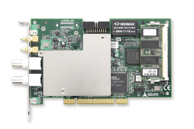
Product Type: 2-Channel, 14-bit, High-Speed PCI Digitizer with Onboard SDRAM
The ADLINK PCI-9820 is a high-resolution, two-channel PCI analog-to-digital (A/D) digitizer designed for high-speed waveform acquisition and signal analysis. It supports simultaneous sampling at up to 65 MS/s per channel and up to 130 MS/s in single-channel “ping-pong” mode. The board integrates deep onboard SDRAM memory (128 MB to 512 MB) and a 3k-sample FIFO buffer, enabling extended waveform capture without being limited by PCI bus bandwidth.
### 2. Key Features
- High-Speed Sampling:
- Up to 65 MS/s per channel (dual-channel mode)
- Up to 130 MS/s in single-channel “ping-pong” mode
- High Resolution:
- 14-bit A/D conversion for precise signal digitization
- Deep Onboard Memory:
- Standard 128 MB SDRAM, expandable to 512 MB
- 3k-sample FIFO for real-time streaming
- Flexible Input Configuration:
- Two simultaneous-sampled single-ended analog channels
- Programmable input ranges: ±1 V or ±5 V
- Selectable input impedance: 50 Ω or 1.5 MΩ
- Wide Bandwidth:
- Analog input bandwidth exceeds 30 MHz (-3 dB)
- Advanced Triggering:
- Supports software, analog, digital, and SSI triggers
- Trigger modes: pre-trigger, post-trigger, middle-trigger, delay-trigger
- Repeated trigger acquisition with minimal rearming interval (2 timebase cycles)
- Multiple Device Synchronization:
- System Synchronization Interface (SSI) for timing and trigger sharing across multiple PCI-9820 boards
- Auto-Calibration:
- Fully automated offset and gain calibration using onboard DACs
- Calibration constants stored in EEPROM
- Software Support:
- Drivers for Windows (WD-DASK), Linux (WD-DASK/X)
- LabVIEW® driver (WD-LVIEW) and ActiveX controls (WD-OCX)
- DAQBench™ ActiveX visualization toolkit
- Compact PCI Form Factor:
- Half-size PCI card supporting both 3.3 V and 5 V signaling environments
### 3. Technical Specifications
Analog Input
- Channels: 2 simultaneous-sampled single-ended
- Resolution: 14 bits
- Sampling Rate:
- 60 MS/s (internal timebase)
- 65 MS/s (external timebase)
- 120 MS/s (ping-pong mode, internal)
- 130 MS/s (ping-pong mode, external)
- Bandwidth (-3 dB): ≥30 MHz
- Input Ranges: ±1 V, ±5 V (software programmable)
- Input Coupling: DC
- Input Impedance: 50 Ω or 1.5 MΩ (solder-selectable)
- Overvoltage Protection:
- ±5 V range: ±14 V
- ±1 V range: ±5 V
- Crosstalk: -80 dB (DC to 1 MHz)
- THD: -75 dB
- SNR: 66 dB (±5 V), 62 dB (±1 V)
- SFDR: 75 dB
- System Noise: 1.25 LSB (±5 V), 1.75 LSB (±1 V)
Memory & Data Transfer
- Onboard SDRAM: 128 MB (standard), up to 512 MB
- FIFO Buffer: 3,056 samples
- Data Transfer: Bus mastering DMA with scatter-gather support
Timebase System
- Internal Clock: 60 MHz
- External Clock Input: SMB connector, 50 Ω AC-coupled
- Input amplitude: 1–2 Vpp
- Frequency range: 500 kHz–65 MHz
- Overvoltage protection: 2.5 Vpp
- SSI Timebase: 60 MHz LVTTL
Triggering
- Sources: Software, analog, digital, SSI
- Modes: Pre-trigger, post-trigger, middle-trigger, delay-trigger
- Analog Trigger:
- Source: CH0 or CH1
- Slope: Rising/falling
- Sensitivity: 256 steps across full-scale range
- Hysteresis: 1.5% FS
- Offset error: 1.25% FS
- Digital Trigger:
- Connector: SMB
- Compatibility: 5 V TTL
- Minimum pulse width: 10–20 ns
- Repeated Trigger Interval: 2 timebase cycles
- Pre/Post Trigger Depth: 64 MB–512 MB (depending on memory size)
Calibration
- Reference Voltage: +5.000 V
- Temperature Drift: ±2 ppm/°C
- Stability: 6 ppm/1000 hours
- Warm-up Time: 15 minutes
General Specifications
- Dimensions: 175 mm × 107 mm (excluding connectors)
- Connectors:
- 2 × BNC (analog inputs)
- 2 × SMB (external trigger and timebase)
- Operating Temperature: 0–50 °C
- Storage Temperature: -20–80 °C
- Humidity: 5–95% RH, non-condensing
- Power Requirements:
- +5 V @ 895 mA
- +12 V @ 295 mA
- +3.3 V @ 310 mA (128 MB) / 430 mA (512 MB)
### 4. Functionality
The PCI-9820 digitizer converts analog signals into high-resolution digital data for analysis and processing. It employs two 14-bit pipeline ADCs operating at up to 65 MS/s per channel. In single-channel “ping-pong” mode, both ADCs interleave to achieve up to 130 MS/s sampling.
Captured data is stored in onboard SDRAM, allowing long-duration waveform recording independent of PCI bus bandwidth. For lower throughput applications, the 3k-sample FIFO enables direct real-time streaming to host memory.
Use Cases and Applications:
- Radar and sonar waveform capture
- Ultrasound and biomedical signal acquisition
- Software-defined radio (SDR)
- RF and transient signal analysis
- Automotive and aerospace testing
- Automated Test Equipment (ATE)
- Laboratory and industrial measurement systems
Compatibility:
- PCI 32-bit, 3.3 V/5 V signaling
- Supported OS: Windows 98/NT/2000/XP, Linux
- Software integration with LabVIEW®, ActiveX, and custom C/C++/VB applications
### 5. Components & Accessories
Included Items:
- PCI-9820 Digitizer Board
- ADLINK All-in-One Software CD
- Software Installation Guide
- User’s Manual
Optional Accessories:
- SMB-SMB-1M: 1-meter SMB-to-SMB cable
- SMB-BNC-1M: 1-meter SMB-to-BNC cable
- ACL-SSI-2: SSI bus cable for 2 devices
- ACL-SSI-3: SSI bus cable for 3 devices
- ACL-SSI-4: SSI bus cable for 4 devices
Connectors:
- CH0, CH1: BNC connectors for analog input
- CLK IN: SMB connector for external timebase input
- TRG IO: SMB connector for external digital trigger I/O
- SSI: 20-pin header for synchronization bus
### 6. Installation & Setup
Installation Requirements:
- Available PCI slot (32-bit, 3.3 V or 5 V)
- Compatible PC with supported OS
- Anti-static handling precautions
Setup Procedure:
1. Power off the host system and insert the PCI-9820 into an available PCI slot.
2. Secure the card and connect required BNC/SMB cables.
3. Install ADLINK drivers and software from the provided CD.
4. Configure input impedance (50 Ω or 1.5 MΩ) via solder jumpers J6 and J7.
5. Use the `PCI_SCAN` utility to verify system recognition.
Mounting Options:
- Standard PCI slot installation
- SSI ribbon cable connection for multi-card synchronization
Configuration:
- Plug-and-play PCI configuration (no manual IRQ/DMA settings)
- Software-based range, trigger, and timebase configuration
### 7. Performance & Capabilities
Sampling Performance:
- Dual-channel simultaneous sampling up to 65 MS/s
- Single-channel interleaved sampling up to 130 MS/s
- 14-bit resolution ensures high dynamic range and low quantization noise
Data Throughput:
- Maximum internal throughput: 240 MB/s (2 channels × 60 MS/s × 2 bytes)
- PCI bus transfer via scatter-gather DMA for efficient large-block data movement
Efficiency & Limitations:
- Real-time streaming limited by PCI bandwidth (132 MB/s)
- Extended recording duration enabled by onboard SDRAM
- Ping-pong mode limited to CH0 for single-channel operation
Signal Integrity:
- Low distortion (THD -75 dB)
- High SNR (up to 66 dB)
- Crosstalk suppression better than -80 dB
Trigger Responsiveness:
- Minimum digital trigger pulse width: 10–20 ns
- Re-trigger interval: 2 timebase cycles
- Analog trigger resolution: 256 discrete levels
### 8. Standards & Compliance
Bus Interface:
- PCI Local Bus Specification, Revision 2.2
- 32-bit, 33 MHz, 3.3 V/5 V signaling
Electrical & Environmental Compliance:
- CE and FCC Class A (industrial environment)
- RoHS-compliant manufacturing
Industry Standards:
- Compatible with ADLINK NuDAQ® and PXI/CompactPCI platforms
- Supports SSI synchronization standard for multi-device timing alignment
### 9. Additional Information
Warranty:
- Standard 2-year limited warranty from ADLINK
- Covers defects in materials and workmanship
- Excludes damage from misuse, improper installation, or environmental factors
Support & Maintenance:
- Technical support via email: service@adlinktech.com
- RMA service available through ADLINK’s website
- Firmware and driver updates downloadable from [www.adlinktech.com](http://www.adlinktech.com)
Maintenance Recommendations:
- Recalibrate after installation or environmental change
- Warm-up for 15 minutes before calibration
- Store in dry, temperature-controlled environment (-20 to 80 °C)
Software Updates & Integration:
- WD-DASK and WD-DASK/X libraries for custom programming
- WD-LVIEW for LabVIEW® integration
- WD-OCX ActiveX controls for VB/VC++ development
- DAQBench™ for GUI-based measurement and automation
### Summary
The ADLINK PCI-9820 is a robust, high-performance PCI digitizer optimized for high-speed, high-resolution signal acquisition. Its dual 14-bit ADCs, deep onboard memory, and flexible triggering make it ideal for demanding applications such as radar, ultrasound, and RF analysis. With comprehensive software support, auto-calibration, and multi-device synchronization, the PCI-9820 provides a complete, scalable solution for laboratory, industrial, and research environments requiring precise, high-speed data acquisition.
Ordering Information:
- PCI-9820D/128-0: 2-CH 65 MS/s 14-bit Digitizer with 128 MB SDRAM
- PCI-9820D/512-0: 2-CH 65 MS/s 14-bit Digitizer with 512 MB SDRAM
Manufacturer Contact:
ADLINK Technology Inc.
9F, No. 166, Jian Yi Road, Chungho City, Taipei 235, Taiwan
Tel: +886-2-82265877 | Fax: +886-2-82265717
Email: service@adlinktech.com

### 1. Product Overview
Product Name: PCI-9820
Model: PCI-9820D/128-0, PCI-9820D/512-0
Series: NuDAQ® PCI Data Acquisition Series
Article Number: PCI-9820
Manufacturer: ADLINK Technology Inc.
Manufacturer Website: [www.adlinktech.com](http://www.adlinktech.com)
Product Type: 2-Channel, 14-bit, High-Speed PCI Digitizer with Onboard SDRAM
The ADLINK PCI-9820 is a high-resolution, two-channel PCI analog-to-digital (A/D) digitizer designed for high-speed waveform acquisition and signal analysis. It supports simultaneous sampling at up to 65 MS/s per channel and up to 130 MS/s in single-channel “ping-pong” mode. The board integrates deep onboard SDRAM memory (128 MB to 512 MB) and a 3k-sample FIFO buffer, enabling extended waveform capture without being limited by PCI bus bandwidth.
### 2. Key Features
- High-Speed Sampling:
- Up to 65 MS/s per channel (dual-channel mode)
- Up to 130 MS/s in single-channel “ping-pong” mode
- High Resolution:
- 14-bit A/D conversion for precise signal digitization
- Deep Onboard Memory:
- Standard 128 MB SDRAM, expandable to 512 MB
- 3k-sample FIFO for real-time streaming
- Flexible Input Configuration:
- Two simultaneous-sampled single-ended analog channels
- Programmable input ranges: ±1 V or ±5 V
- Selectable input impedance: 50 Ω or 1.5 MΩ
- Wide Bandwidth:
- Analog input bandwidth exceeds 30 MHz (-3 dB)
- Advanced Triggering:
- Supports software, analog, digital, and SSI triggers
- Trigger modes: pre-trigger, post-trigger, middle-trigger, delay-trigger
- Repeated trigger acquisition with minimal rearming interval (2 timebase cycles)
- Multiple Device Synchronization:
- System Synchronization Interface (SSI) for timing and trigger sharing across multiple PCI-9820 boards
- Auto-Calibration:
- Fully automated offset and gain calibration using onboard DACs
- Calibration constants stored in EEPROM
- Software Support:
- Drivers for Windows (WD-DASK), Linux (WD-DASK/X)
- LabVIEW® driver (WD-LVIEW) and ActiveX controls (WD-OCX)
- DAQBench™ ActiveX visualization toolkit
- Compact PCI Form Factor:
- Half-size PCI card supporting both 3.3 V and 5 V signaling environments
### 3. Technical Specifications
Analog Input
- Channels: 2 simultaneous-sampled single-ended
- Resolution: 14 bits
- Sampling Rate:
- 60 MS/s (internal timebase)
- 65 MS/s (external timebase)
- 120 MS/s (ping-pong mode, internal)
- 130 MS/s (ping-pong mode, external)
- Bandwidth (-3 dB): ≥30 MHz
- Input Ranges: ±1 V, ±5 V (software programmable)
- Input Coupling: DC
- Input Impedance: 50 Ω or 1.5 MΩ (solder-selectable)
- Overvoltage Protection:
- ±5 V range: ±14 V
- ±1 V range: ±5 V
- Crosstalk: -80 dB (DC to 1 MHz)
- THD: -75 dB
- SNR: 66 dB (±5 V), 62 dB (±1 V)
- SFDR: 75 dB
- System Noise: 1.25 LSB (±5 V), 1.75 LSB (±1 V)
Memory & Data Transfer
- Onboard SDRAM: 128 MB (standard), up to 512 MB
- FIFO Buffer: 3,056 samples
- Data Transfer: Bus mastering DMA with scatter-gather support
Timebase System
- Internal Clock: 60 MHz
- External Clock Input: SMB connector, 50 Ω AC-coupled
- Input amplitude: 1–2 Vpp
- Frequency range: 500 kHz–65 MHz
- Overvoltage protection: 2.5 Vpp
- SSI Timebase: 60 MHz LVTTL
Triggering
- Sources: Software, analog, digital, SSI
- Modes: Pre-trigger, post-trigger, middle-trigger, delay-trigger
- Analog Trigger:
- Source: CH0 or CH1
- Slope: Rising/falling
- Sensitivity: 256 steps across full-scale range
- Hysteresis: 1.5% FS
- Offset error: 1.25% FS
- Digital Trigger:
- Connector: SMB
- Compatibility: 5 V TTL
- Minimum pulse width: 10–20 ns
- Repeated Trigger Interval: 2 timebase cycles
- Pre/Post Trigger Depth: 64 MB–512 MB (depending on memory size)
Calibration
- Reference Voltage: +5.000 V
- Temperature Drift: ±2 ppm/°C
- Stability: 6 ppm/1000 hours
- Warm-up Time: 15 minutes
General Specifications
- Dimensions: 175 mm × 107 mm (excluding connectors)
- Connectors:
- 2 × BNC (analog inputs)
- 2 × SMB (external trigger and timebase)
- Operating Temperature: 0–50 °C
- Storage Temperature: -20–80 °C
- Humidity: 5–95% RH, non-condensing
- Power Requirements:
- +5 V @ 895 mA
- +12 V @ 295 mA
- +3.3 V @ 310 mA (128 MB) / 430 mA (512 MB)
### 4. Functionality
The PCI-9820 digitizer converts analog signals into high-resolution digital data for analysis and processing. It employs two 14-bit pipeline ADCs operating at up to 65 MS/s per channel. In single-channel “ping-pong” mode, both ADCs interleave to achieve up to 130 MS/s sampling.
Captured data is stored in onboard SDRAM, allowing long-duration waveform recording independent of PCI bus bandwidth. For lower throughput applications, the 3k-sample FIFO enables direct real-time streaming to host memory.
Use Cases and Applications:
- Radar and sonar waveform capture
- Ultrasound and biomedical signal acquisition
- Software-defined radio (SDR)
- RF and transient signal analysis
- Automotive and aerospace testing
- Automated Test Equipment (ATE)
- Laboratory and industrial measurement systems
Compatibility:
- PCI 32-bit, 3.3 V/5 V signaling
- Supported OS: Windows 98/NT/2000/XP, Linux
- Software integration with LabVIEW®, ActiveX, and custom C/C++/VB applications
### 5. Components & Accessories
Included Items:
- PCI-9820 Digitizer Board
- ADLINK All-in-One Software CD
- Software Installation Guide
- User’s Manual
Optional Accessories:
- SMB-SMB-1M: 1-meter SMB-to-SMB cable
- SMB-BNC-1M: 1-meter SMB-to-BNC cable
- ACL-SSI-2: SSI bus cable for 2 devices
- ACL-SSI-3: SSI bus cable for 3 devices
- ACL-SSI-4: SSI bus cable for 4 devices
Connectors:
- CH0, CH1: BNC connectors for analog input
- CLK IN: SMB connector for external timebase input
- TRG IO: SMB connector for external digital trigger I/O
- SSI: 20-pin header for synchronization bus
### 6. Installation & Setup
Installation Requirements:
- Available PCI slot (32-bit, 3.3 V or 5 V)
- Compatible PC with supported OS
- Anti-static handling precautions
Setup Procedure:
1. Power off the host system and insert the PCI-9820 into an available PCI slot.
2. Secure the card and connect required BNC/SMB cables.
3. Install ADLINK drivers and software from the provided CD.
4. Configure input impedance (50 Ω or 1.5 MΩ) via solder jumpers J6 and J7.
5. Use the `PCI_SCAN` utility to verify system recognition.
Mounting Options:
- Standard PCI slot installation
- SSI ribbon cable connection for multi-card synchronization
Configuration:
- Plug-and-play PCI configuration (no manual IRQ/DMA settings)
- Software-based range, trigger, and timebase configuration
### 7. Performance & Capabilities
Sampling Performance:
- Dual-channel simultaneous sampling up to 65 MS/s
- Single-channel interleaved sampling up to 130 MS/s
- 14-bit resolution ensures high dynamic range and low quantization noise
Data Throughput:
- Maximum internal throughput: 240 MB/s (2 channels × 60 MS/s × 2 bytes)
- PCI bus transfer via scatter-gather DMA for efficient large-block data movement
Efficiency & Limitations:
- Real-time streaming limited by PCI bandwidth (132 MB/s)
- Extended recording duration enabled by onboard SDRAM
- Ping-pong mode limited to CH0 for single-channel operation
Signal Integrity:
- Low distortion (THD -75 dB)
- High SNR (up to 66 dB)
- Crosstalk suppression better than -80 dB
Trigger Responsiveness:
- Minimum digital trigger pulse width: 10–20 ns
- Re-trigger interval: 2 timebase cycles
- Analog trigger resolution: 256 discrete levels
### 8. Standards & Compliance
Bus Interface:
- PCI Local Bus Specification, Revision 2.2
- 32-bit, 33 MHz, 3.3 V/5 V signaling
Electrical & Environmental Compliance:
- CE and FCC Class A (industrial environment)
- RoHS-compliant manufacturing
Industry Standards:
- Compatible with ADLINK NuDAQ® and PXI/CompactPCI platforms
- Supports SSI synchronization standard for multi-device timing alignment
### 9. Additional Information
Warranty:
- Standard 2-year limited warranty from ADLINK
- Covers defects in materials and workmanship
- Excludes damage from misuse, improper installation, or environmental factors
Support & Maintenance:
- Technical support via email: service@adlinktech.com
- RMA service available through ADLINK’s website
- Firmware and driver updates downloadable from [www.adlinktech.com](http://www.adlinktech.com)
Maintenance Recommendations:
- Recalibrate after installation or environmental change
- Warm-up for 15 minutes before calibration
- Store in dry, temperature-controlled environment (-20 to 80 °C)
Software Updates & Integration:
- WD-DASK and WD-DASK/X libraries for custom programming
- WD-LVIEW for LabVIEW® integration
- WD-OCX ActiveX controls for VB/VC++ development
- DAQBench™ for GUI-based measurement and automation
### Summary
The ADLINK PCI-9820 is a robust, high-performance PCI digitizer optimized for high-speed, high-resolution signal acquisition. Its dual 14-bit ADCs, deep onboard memory, and flexible triggering make it ideal for demanding applications such as radar, ultrasound, and RF analysis. With comprehensive software support, auto-calibration, and multi-device synchronization, the PCI-9820 provides a complete, scalable solution for laboratory, industrial, and research environments requiring precise, high-speed data acquisition.
Ordering Information:
- PCI-9820D/128-0: 2-CH 65 MS/s 14-bit Digitizer with 128 MB SDRAM
- PCI-9820D/512-0: 2-CH 65 MS/s 14-bit Digitizer with 512 MB SDRAM
Manufacturer Contact:
ADLINK Technology Inc.
9F, No. 166, Jian Yi Road, Chungho City, Taipei 235, Taiwan
Tel: +886-2-82265877 | Fax: +886-2-82265717
Email: service@adlinktech.com

-
05-02.pdf
PDF Catalog
-
PCI-9820_Datasheet_2.pdf
PDF Catalog
-
PCI-9820_Manual_2.pdf
Manual
-
PCI-9820_Manual_1.pdf
Manual
- WD-DASK - Windows driver API for PCI/PXI-9820 and PXI-98xx Digitizer
- SMB-BNC-1m - SMB to BNC cable 1m (PXI-9816/26/46)