DIN-68H-01
LOOKING FOR THE RIGHT
INDUSTRIAL SOLUTION?
Discover embedded, communication and automation solutions tailored to your application.
- High-Speed PCI Express Interface:
Utilizes a PCI Express x4 lane interface providing up to 400 MB/s throughput.
- Flexible Channel Configuration:
32 bi-directional digital I/O channels divided into four 8-bit groups, each configurable as input or output.
- Selectable Logic Levels:
Software-selectable voltage levels of 1.8 V, 2.5 V, or 3.3 V (5 V compatible) for all I/O lines.
- High Clock Rates:
- Internal clock up to 100 MHz
- External clock up to 200 MHz (DI mode, 8/16-bit width)
- Phase Shift Control:
80-step phase shifting (4.5° per step) for precise timing alignment in external clock mode.
- Integrated Serial Interfaces:
Built-in I²C and SPI master interfaces for direct communication with peripheral devices.
- DMA and FIFO Architecture:
Scatter-gather bus-mastering DMA with 8K-sample DI FIFO and 20K-sample DO FIFO ensures continuous high-speed data transfer without CPU overhead.
- Trigger and Handshake Support:
Multiple trigger modes (post, gated, re-trigger) and handshake protocols for synchronized data exchange.
- Auxiliary Function I/O (AFI):
Eight programmable AFI lines supporting static I/O, triggers, handshake, and clock I/O.
- Software Compatibility:
Supports Windows XP/7/8 (x86/x64) and Linux; compatible with LabVIEW®, MATLAB®, and Visual Studio .NET.
Utilizes a PCI Express x4 lane interface providing up to 400 MB/s throughput.
- Flexible Channel Configuration:
32 bi-directional digital I/O channels divided into four 8-bit groups, each configurable as input or output.
- Selectable Logic Levels:
Software-selectable voltage levels of 1.8 V, 2.5 V, or 3.3 V (5 V compatible) for all I/O lines.
- High Clock Rates:
- Internal clock up to 100 MHz
- External clock up to 200 MHz (DI mode, 8/16-bit width)
- Phase Shift Control:
80-step phase shifting (4.5° per step) for precise timing alignment in external clock mode.
- Integrated Serial Interfaces:
Built-in I²C and SPI master interfaces for direct communication with peripheral devices.
- DMA and FIFO Architecture:
Scatter-gather bus-mastering DMA with 8K-sample DI FIFO and 20K-sample DO FIFO ensures continuous high-speed data transfer without CPU overhead.
- Trigger and Handshake Support:
Multiple trigger modes (post, gated, re-trigger) and handshake protocols for synchronized data exchange.
- Auxiliary Function I/O (AFI):
Eight programmable AFI lines supporting static I/O, triggers, handshake, and clock I/O.
- Software Compatibility:
Supports Windows XP/7/8 (x86/x64) and Linux; compatible with LabVIEW®, MATLAB®, and Visual Studio .NET.
Comprehensive Product Summary: ADLINK PCIe-7360 High-Speed Digital I/O Card
### 1. Product Overview
Product Name: PCIe-7360
Model: PCIe-7360
Series: High-Speed Digital I/O (DIO) PCI Express Series
Article Number: PCIe-7360
Manufacturer: ADLINK Technology, Inc.
Part Number: 50-11042-1000
Manual Revision: 2.00 (August 2, 2013)
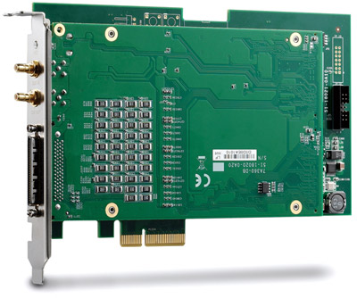
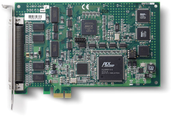
The ADLINK PCIe-7360 is a high-performance, 32-channel, bi-directional digital I/O card designed for PCI Express® x4 interfaces. It supports data throughput up to 400 MB/s and clock rates up to 100 MHz (internal) or 200 MHz (external). The card is optimized for high-speed digital data acquisition, pattern generation, and real-time communication with external devices in applications such as IC testing, digital imaging, and automated test equipment (ATE).
### 2. Key Features
- High-Speed PCI Express Interface:
Utilizes a PCI Express x4 lane interface providing up to 400 MB/s throughput.
- Flexible Channel Configuration:
32 bi-directional digital I/O channels divided into four 8-bit groups, each configurable as input or output.
- Selectable Logic Levels:
Software-selectable voltage levels of 1.8 V, 2.5 V, or 3.3 V (5 V compatible) for all I/O lines.
- High Clock Rates:
- Internal clock up to 100 MHz
- External clock up to 200 MHz (DI mode, 8/16-bit width)
- Phase Shift Control:
80-step phase shifting (4.5° per step) for precise timing alignment in external clock mode.
- Integrated Serial Interfaces:
Built-in I²C and SPI master interfaces for direct communication with peripheral devices.
- DMA and FIFO Architecture:
Scatter-gather bus-mastering DMA with 8K-sample DI FIFO and 20K-sample DO FIFO ensures continuous high-speed data transfer without CPU overhead.
- Trigger and Handshake Support:
Multiple trigger modes (post, gated, re-trigger) and handshake protocols for synchronized data exchange.
- Auxiliary Function I/O (AFI):
Eight programmable AFI lines supporting static I/O, triggers, handshake, and clock I/O.
- Software Compatibility:
Supports Windows XP/7/8 (x86/x64) and Linux; compatible with LabVIEW®, MATLAB®, and Visual Studio .NET.
### 3. Technical Specifications
Interface: PCI Express x4
Connectors:
- 68-pin SCSI-VHDCI (for 32-bit data and 8 AFI lines)
- 2 × SMB jacks (CLK IN and CLK OUT)
Dimensions: 168 mm (L) × 112 mm (H)
Operating Temperature: 0°C to 55°C
Storage Temperature: -20°C to 70°C
Humidity: 5–95% non-condensing
Power Consumption:
- +3.3 VDC: 860 mA (typ.), 950 mA (max)
- +12 VDC: 270 mA (typ.), 550 mA (max)
- Total: 6.1 W (typ.), 9.8 W (max)
Digital I/O:
- 32 channels, grouped in 4 × 8-bit ports
- Direction: Programmable per group
- Logic levels: 1.8 V / 2.5 V / 3.3 V (software selectable)
- Input impedance: 10 kΩ
- Output impedance: 50 Ω
- Input protection: -1 V to +6 V
- Output protection: -0.5 V to +3.8 V
- Max throughput: 400 MB/s (DI/DO)
- Output drive: ±8 mA (1.8 V), ±16 mA (2.5 V), ±32 mA (3.3 V)
Timing Accuracy:
- Channel-to-channel skew: ±1.08 ns
- Setup/Hold time: 2 ns each
- Clock jitter: 300 ps
- Duty cycle: 50%
Clocking:
- Internal: 100 MHz oscillator (programmable divider 1–65535)
- External: Up to 200 MHz (DI), 100 MHz (DO)
- Phase shift: 80 steps (4.5° per step)
AFI (Application Function I/O):
- 8 channels, programmable direction
- Logic levels: 1.8 V / 2.5 V / 3.3 V
- Supported modes: I²C, SPI, handshake, trigger, clock I/O
- Input impedance: 10 kΩ
- Output impedance: 50 Ω
### 4. Functionality
The PCIe-7360 functions as a high-speed digital interface for data acquisition and generation. It supports multiple operational modes:
- Digital Input (DI): Captures high-speed digital signals from external devices using internal or external clocks.
- Digital Output (DO): Generates programmable digital patterns for device testing or simulation.
- Clock Synchronization: Internal or external clock sources with optional phase shifting for precise timing.
- Triggering: Supports software and external triggers with post, gated, and re-trigger modes.
- Handshake Modes: Ensures reliable data transfer with DI/DO request and acknowledge signals.
- Serial Communication: Built-in I²C and SPI master interfaces for direct peripheral control.
- Pattern Match & COS Detection: Detects specific digital patterns or state changes and generates interrupts or event outputs.
Applications:
- IC and semiconductor testing
- Digital pattern generation/acquisition
- High-speed data exchange
- Interface to external ADC/DAC modules
- Automated Test Equipment (ATE)
- Digital image capture and video playback systems
Compatibility:
- Operating Systems: Windows XP/7/8 (x86/x64), Linux
- Software: LabVIEW®, MATLAB®, Visual Studio .NET
- Drivers: DAQPilot SDK, PCIS-DASK kernel drivers
### 5. Components & Accessories
Included Items:
- PCIe-7360 DIO card
- ADLINK All-in-One CD (drivers, SDKs, documentation)
- Quick Start Guide
Optional Accessories:
- DIN-68H-01: Terminal board with 68-pin SCSI-VHDCI connector, 0/50 Ω jumper-selectable impedance.
- ACL-10279: 68-pin SCSI-VHDCI cable (50 Ω impedance).
- SMB-SMB-1M: 1-meter SMB-to-SMB cable for clock I/O.
- SMB-BNC-1M: 1-meter SMB-to-BNC cable for clock I/O.
Connectors:
- 68-pin SCSI-VHDCI for data and AFI lines
- 2 × SMB jacks for CLK IN/OUT
### 6. Installation & Setup
Requirements:
- Available PCI Express x4 slot
- Supported OS and driver installation prior to hardware insertion
Installation Steps:
1. Power off the system and remove the chassis cover.
2. Insert the PCIe-7360 into an available PCIe x4 slot.
3. Secure the card with a screw.
4. Reassemble the chassis and power on the system.
5. Install ADLINK drivers and verify device recognition.
Configuration:
- No jumper settings required; Plug-and-Play configuration via BIOS and OS.
- Software-configurable logic levels and I/O directions.
Cabling & Termination:
- Use 50 Ω impedance cables (ACL-10279) for high-speed signal integrity.
- DIN-68H termination board recommended for impedance matching and signal quality.
### 7. Performance & Capabilities
- Throughput: Up to 400 MB/s sustained transfer rate
- Clock Rates:
- Internal: 100 MHz (programmable divider)
- External: 200 MHz (DI), 100 MHz (DO)
- FIFO Buffers:
- DI: 8K samples
- DO: 20K samples
- DMA: Scatter-gather bus-mastering DMA for continuous data streaming
- Phase Shift: 80-step (4.5° increments) for timing optimization
- Trigger Latency:
- External trigger to data output: ~5 cycles
- Software trigger to data output: ~4 cycles
- Handshake Timing:
- DI/DO request-acknowledge cycle: 40–50 ns typical
- Pattern Match & COS:
- Pattern match on logic level or edge transitions
- COS detection at 125 MHz sampling rate (8 ns resolution)
Limitations:
- External clock phase shift available only for continuous free-running clocks (20–100 MHz).
- External 200 MHz operation limited to 8/16-bit DI width.
### 8. Standards & Compliance
- Bus Interface: PCI Express® x4 compliant
- Environmental Compliance:
- RoHS (Restriction of Hazardous Substances)
- WEEE (Waste Electrical and Electronic Equipment)
- Safety: Designed for industrial and laboratory environments
- Operating Standards:
- CE and FCC Class A (industrial use)
- ESD protection on I/O lines
### 9. Additional Information
Warranty & Support:
- Standard manufacturer warranty (contact ADLINK for terms)
- Global technical support via regional offices in Taiwan, USA, China, Japan, Korea, Singapore, India, Israel, and Europe
Maintenance:
- Handle in static-free environments
- Avoid exposure to moisture and high temperatures
- Use anti-static packaging for storage and transport
Software Updates:
- DAQPilot SDK and PCIS-DASK driver updates available from ADLINK’s website
- Latest versions required for full PCIe-7360 compatibility (DAQPilot ≥ 2.6.1.0705, PCIS-DASK ≥ 5.10)
Environmental Responsibility:
ADLINK ensures compliance with EU environmental directives and encourages proper recycling and disposal of electronic components.
### Summary
The ADLINK PCIe-7360 is a robust, high-speed digital I/O solution engineered for demanding data acquisition and generation tasks. With its 32 programmable channels, 400 MB/s throughput, and flexible clocking and triggering architecture, it provides precise control and synchronization for high-performance test and measurement systems. Its integrated I²C/SPI interfaces, advanced DMA engine, and software ecosystem make it ideal for developers and engineers requiring deterministic, high-bandwidth digital interfacing in industrial, research, and automated testing environments.

### 1. Product Overview
Product Name: PCIe-7360
Model: PCIe-7360
Series: High-Speed Digital I/O (DIO) PCI Express Series
Article Number: PCIe-7360
Manufacturer: ADLINK Technology, Inc.
Part Number: 50-11042-1000
Manual Revision: 2.00 (August 2, 2013)
The ADLINK PCIe-7360 is a high-performance, 32-channel, bi-directional digital I/O card designed for PCI Express® x4 interfaces. It supports data throughput up to 400 MB/s and clock rates up to 100 MHz (internal) or 200 MHz (external). The card is optimized for high-speed digital data acquisition, pattern generation, and real-time communication with external devices in applications such as IC testing, digital imaging, and automated test equipment (ATE).
### 2. Key Features
- High-Speed PCI Express Interface:
Utilizes a PCI Express x4 lane interface providing up to 400 MB/s throughput.
- Flexible Channel Configuration:
32 bi-directional digital I/O channels divided into four 8-bit groups, each configurable as input or output.
- Selectable Logic Levels:
Software-selectable voltage levels of 1.8 V, 2.5 V, or 3.3 V (5 V compatible) for all I/O lines.
- High Clock Rates:
- Internal clock up to 100 MHz
- External clock up to 200 MHz (DI mode, 8/16-bit width)
- Phase Shift Control:
80-step phase shifting (4.5° per step) for precise timing alignment in external clock mode.
- Integrated Serial Interfaces:
Built-in I²C and SPI master interfaces for direct communication with peripheral devices.
- DMA and FIFO Architecture:
Scatter-gather bus-mastering DMA with 8K-sample DI FIFO and 20K-sample DO FIFO ensures continuous high-speed data transfer without CPU overhead.
- Trigger and Handshake Support:
Multiple trigger modes (post, gated, re-trigger) and handshake protocols for synchronized data exchange.
- Auxiliary Function I/O (AFI):
Eight programmable AFI lines supporting static I/O, triggers, handshake, and clock I/O.
- Software Compatibility:
Supports Windows XP/7/8 (x86/x64) and Linux; compatible with LabVIEW®, MATLAB®, and Visual Studio .NET.
### 3. Technical Specifications
Interface: PCI Express x4
Connectors:
- 68-pin SCSI-VHDCI (for 32-bit data and 8 AFI lines)
- 2 × SMB jacks (CLK IN and CLK OUT)
Dimensions: 168 mm (L) × 112 mm (H)
Operating Temperature: 0°C to 55°C
Storage Temperature: -20°C to 70°C
Humidity: 5–95% non-condensing
Power Consumption:
- +3.3 VDC: 860 mA (typ.), 950 mA (max)
- +12 VDC: 270 mA (typ.), 550 mA (max)
- Total: 6.1 W (typ.), 9.8 W (max)
Digital I/O:
- 32 channels, grouped in 4 × 8-bit ports
- Direction: Programmable per group
- Logic levels: 1.8 V / 2.5 V / 3.3 V (software selectable)
- Input impedance: 10 kΩ
- Output impedance: 50 Ω
- Input protection: -1 V to +6 V
- Output protection: -0.5 V to +3.8 V
- Max throughput: 400 MB/s (DI/DO)
- Output drive: ±8 mA (1.8 V), ±16 mA (2.5 V), ±32 mA (3.3 V)
Timing Accuracy:
- Channel-to-channel skew: ±1.08 ns
- Setup/Hold time: 2 ns each
- Clock jitter: 300 ps
- Duty cycle: 50%
Clocking:
- Internal: 100 MHz oscillator (programmable divider 1–65535)
- External: Up to 200 MHz (DI), 100 MHz (DO)
- Phase shift: 80 steps (4.5° per step)
AFI (Application Function I/O):
- 8 channels, programmable direction
- Logic levels: 1.8 V / 2.5 V / 3.3 V
- Supported modes: I²C, SPI, handshake, trigger, clock I/O
- Input impedance: 10 kΩ
- Output impedance: 50 Ω
### 4. Functionality
The PCIe-7360 functions as a high-speed digital interface for data acquisition and generation. It supports multiple operational modes:
- Digital Input (DI): Captures high-speed digital signals from external devices using internal or external clocks.
- Digital Output (DO): Generates programmable digital patterns for device testing or simulation.
- Clock Synchronization: Internal or external clock sources with optional phase shifting for precise timing.
- Triggering: Supports software and external triggers with post, gated, and re-trigger modes.
- Handshake Modes: Ensures reliable data transfer with DI/DO request and acknowledge signals.
- Serial Communication: Built-in I²C and SPI master interfaces for direct peripheral control.
- Pattern Match & COS Detection: Detects specific digital patterns or state changes and generates interrupts or event outputs.
Applications:
- IC and semiconductor testing
- Digital pattern generation/acquisition
- High-speed data exchange
- Interface to external ADC/DAC modules
- Automated Test Equipment (ATE)
- Digital image capture and video playback systems
Compatibility:
- Operating Systems: Windows XP/7/8 (x86/x64), Linux
- Software: LabVIEW®, MATLAB®, Visual Studio .NET
- Drivers: DAQPilot SDK, PCIS-DASK kernel drivers
### 5. Components & Accessories
Included Items:
- PCIe-7360 DIO card
- ADLINK All-in-One CD (drivers, SDKs, documentation)
- Quick Start Guide
Optional Accessories:
- DIN-68H-01: Terminal board with 68-pin SCSI-VHDCI connector, 0/50 Ω jumper-selectable impedance.
- ACL-10279: 68-pin SCSI-VHDCI cable (50 Ω impedance).
- SMB-SMB-1M: 1-meter SMB-to-SMB cable for clock I/O.
- SMB-BNC-1M: 1-meter SMB-to-BNC cable for clock I/O.
Connectors:
- 68-pin SCSI-VHDCI for data and AFI lines
- 2 × SMB jacks for CLK IN/OUT
### 6. Installation & Setup
Requirements:
- Available PCI Express x4 slot
- Supported OS and driver installation prior to hardware insertion
Installation Steps:
1. Power off the system and remove the chassis cover.
2. Insert the PCIe-7360 into an available PCIe x4 slot.
3. Secure the card with a screw.
4. Reassemble the chassis and power on the system.
5. Install ADLINK drivers and verify device recognition.
Configuration:
- No jumper settings required; Plug-and-Play configuration via BIOS and OS.
- Software-configurable logic levels and I/O directions.
Cabling & Termination:
- Use 50 Ω impedance cables (ACL-10279) for high-speed signal integrity.
- DIN-68H termination board recommended for impedance matching and signal quality.
### 7. Performance & Capabilities
- Throughput: Up to 400 MB/s sustained transfer rate
- Clock Rates:
- Internal: 100 MHz (programmable divider)
- External: 200 MHz (DI), 100 MHz (DO)
- FIFO Buffers:
- DI: 8K samples
- DO: 20K samples
- DMA: Scatter-gather bus-mastering DMA for continuous data streaming
- Phase Shift: 80-step (4.5° increments) for timing optimization
- Trigger Latency:
- External trigger to data output: ~5 cycles
- Software trigger to data output: ~4 cycles
- Handshake Timing:
- DI/DO request-acknowledge cycle: 40–50 ns typical
- Pattern Match & COS:
- Pattern match on logic level or edge transitions
- COS detection at 125 MHz sampling rate (8 ns resolution)
Limitations:
- External clock phase shift available only for continuous free-running clocks (20–100 MHz).
- External 200 MHz operation limited to 8/16-bit DI width.
### 8. Standards & Compliance
- Bus Interface: PCI Express® x4 compliant
- Environmental Compliance:
- RoHS (Restriction of Hazardous Substances)
- WEEE (Waste Electrical and Electronic Equipment)
- Safety: Designed for industrial and laboratory environments
- Operating Standards:
- CE and FCC Class A (industrial use)
- ESD protection on I/O lines
### 9. Additional Information
Warranty & Support:
- Standard manufacturer warranty (contact ADLINK for terms)
- Global technical support via regional offices in Taiwan, USA, China, Japan, Korea, Singapore, India, Israel, and Europe
Maintenance:
- Handle in static-free environments
- Avoid exposure to moisture and high temperatures
- Use anti-static packaging for storage and transport
Software Updates:
- DAQPilot SDK and PCIS-DASK driver updates available from ADLINK’s website
- Latest versions required for full PCIe-7360 compatibility (DAQPilot ≥ 2.6.1.0705, PCIS-DASK ≥ 5.10)
Environmental Responsibility:
ADLINK ensures compliance with EU environmental directives and encourages proper recycling and disposal of electronic components.
### Summary
The ADLINK PCIe-7360 is a robust, high-speed digital I/O solution engineered for demanding data acquisition and generation tasks. With its 32 programmable channels, 400 MB/s throughput, and flexible clocking and triggering architecture, it provides precise control and synchronization for high-performance test and measurement systems. Its integrated I²C/SPI interfaces, advanced DMA engine, and software ecosystem make it ideal for developers and engineers requiring deterministic, high-bandwidth digital interfacing in industrial, research, and automated testing environments.
-
PCIe-7360_Datasheet_20130731.pdf
PDF Catalog

- DIN-68H-01 - 68pin term. board 50 Ohm DIN rail (PCIe-7350) w/o cable
- ACL-10279-1 - Cable 1m 68pin 50Ohm impedance (PCIe-7350)
- ACL-10279-3 - Cable 3m 68pin 50Ohm impedance (PCIe-7350)
- SMB-SMB-1m - SMB to SMB cable 1m (PCIe-7350)