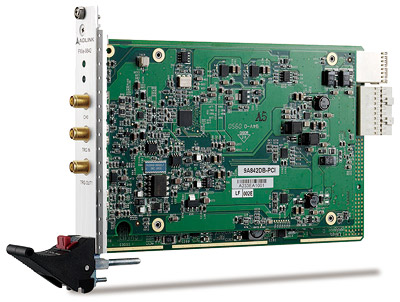
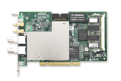
WD-DASK
LOOKING FOR THE RIGHT
INDUSTRIAL SOLUTION?
Discover embedded, communication and automation solutions tailored to your application.
- High Sampling Rate: Up to 200 MS/s real‑time sampling for single‑channel analog input.
- High Resolution: 14‑bit ADC providing 1 in 16,384 quantization levels for precise signal representation.
- Input Range & Impedance: ±1 V input range, 50 Ω ± 2 % impedance, DC‑coupled input.
- Wide Bandwidth: Analog input bandwidth of 100 MHz (‑3 dB).
- High‑Speed Interface: PCI Express x4 or PXIe x4 bus interface supporting sustained data throughput up to 400 MB/s.
- Onboard Memory: 16 K‑sample FIFO buffer for temporary data storage.
- Triggering: Supports software and external digital triggers; post‑trigger, delay‑trigger, and re‑trigger modes.
- Auto‑Calibration: Built‑in reference circuit with ±5 ppm/°C drift for automatic offset and gain calibration.
- Scatter‑Gather DMA: High‑speed, continuous data streaming using bus‑mastering DMA with scatter‑gather capability.
- Auxiliary Digital I/O: 8‑bit static DIO or 2‑bit synchronous digital input (SDI) for mixed‑signal acquisition.
- Software Support: Compatible with Windows and Linux; drivers for LabVIEW, MATLAB, and ADLINK DAQPilot.
- Compact Design: Standard short PCIe card dimensions (106.7 mm × 174.6 mm).
- Connectivity: Three SMA connectors for analog input, external trigger input, and trigger output.
- Certifications: CE, FCC Class A, and full EMC/EMI compliance.
- High Resolution: 14‑bit ADC providing 1 in 16,384 quantization levels for precise signal representation.
- Input Range & Impedance: ±1 V input range, 50 Ω ± 2 % impedance, DC‑coupled input.
- Wide Bandwidth: Analog input bandwidth of 100 MHz (‑3 dB).
- High‑Speed Interface: PCI Express x4 or PXIe x4 bus interface supporting sustained data throughput up to 400 MB/s.
- Onboard Memory: 16 K‑sample FIFO buffer for temporary data storage.
- Triggering: Supports software and external digital triggers; post‑trigger, delay‑trigger, and re‑trigger modes.
- Auto‑Calibration: Built‑in reference circuit with ±5 ppm/°C drift for automatic offset and gain calibration.
- Scatter‑Gather DMA: High‑speed, continuous data streaming using bus‑mastering DMA with scatter‑gather capability.
- Auxiliary Digital I/O: 8‑bit static DIO or 2‑bit synchronous digital input (SDI) for mixed‑signal acquisition.
- Software Support: Compatible with Windows and Linux; drivers for LabVIEW, MATLAB, and ADLINK DAQPilot.
- Compact Design: Standard short PCIe card dimensions (106.7 mm × 174.6 mm).
- Connectivity: Three SMA connectors for analog input, external trigger input, and trigger output.
- Certifications: CE, FCC Class A, and full EMC/EMI compliance.
Comprehensive Product Summary – ADLINK PXIe‑9842 / PCIe‑9842 High‑Speed Digitizer
### 1. Product Overview
Product Name: PXIe‑9842 (also marketed as PCIe‑9842)
Model: PXIe‑9842
Series: PXIe/PCIe High‑Speed Digitizer Series
Article Number: PXIe‑9842
Manufacturer: ADLINK Technology Inc.
Product Type: 200 MS/s, 14‑bit, single‑channel high‑speed analog‑to‑digital (A/D) acquisition card
Form Factor: PXIe x4 or PCI Express x4 interface card
Category: Digitizer / Data Acquisition (DAQ) Module
The ADLINK PXIe‑9842 (equivalent to PCIe‑9842) is a high‑performance single‑channel digitizer designed for precision, high‑speed analog signal acquisition. It integrates a 14‑bit analog‑to‑digital converter (ADC) capable of sampling up to 200 MS/s, with a 100 MHz analog bandwidth and ±1 V input range. The module is optimized for applications requiring accurate, real‑time data capture and streaming, such as radar signal acquisition, optical fiber testing, LIDAR, and scientific instrumentation.
### 2. Key Features
- High Sampling Rate: Up to 200 MS/s real‑time sampling for single‑channel analog input.
- High Resolution: 14‑bit ADC providing 1 in 16,384 quantization levels for precise signal representation.
- Input Range & Impedance: ±1 V input range, 50 Ω ± 2 % impedance, DC‑coupled input.
- Wide Bandwidth: Analog input bandwidth of 100 MHz (‑3 dB).
- High‑Speed Interface: PCI Express x4 or PXIe x4 bus interface supporting sustained data throughput up to 400 MB/s.
- Onboard Memory: 16 K‑sample FIFO buffer for temporary data storage.
- Triggering: Supports software and external digital triggers; post‑trigger, delay‑trigger, and re‑trigger modes.
- Auto‑Calibration: Built‑in reference circuit with ±5 ppm/°C drift for automatic offset and gain calibration.
- Scatter‑Gather DMA: High‑speed, continuous data streaming using bus‑mastering DMA with scatter‑gather capability.
- Auxiliary Digital I/O: 8‑bit static DIO or 2‑bit synchronous digital input (SDI) for mixed‑signal acquisition.
- Software Support: Compatible with Windows and Linux; drivers for LabVIEW, MATLAB, and ADLINK DAQPilot.
- Compact Design: Standard short PCIe card dimensions (106.7 mm × 174.6 mm).
- Connectivity: Three SMA connectors for analog input, external trigger input, and trigger output.
- Certifications: CE, FCC Class A, and full EMC/EMI compliance.
### 3. Technical Specifications
Analog Input
- Channels: 1 (single‑ended)
- Connector Type: SMA screw type
- Input Impedance: 50 Ω ± 2 %
- Input Coupling: DC
- Input Range: ±1.0 V
- Overvoltage Protection: ±5 V
- ADC Resolution: 14 bits (1 in 16,384)
- Offset Error: ±1 mV
- Gain Error: ±0.5 % of input
- Bandwidth (‑3 dB): 100 MHz
- Signal‑to‑Noise Ratio (typical): up to 70 dB with 10 MHz sine input
Timebase
- Clock Source: Internal onboard oscillator
- Frequency: 200 MHz
- Sampling Rate Range: 200 MS/s to 3.051 kS/s
- Timebase Accuracy: ±25 ppm
Trigger System
- Sources: Software or external digital trigger
- Modes: Post‑trigger, delay‑trigger, re‑trigger
- External Trigger Input: 3.3 V TTL (5 V tolerant), 50 Ω impedance
- VIH ≥ 2.0 V, VIL ≤ 0.8 V, max input –0.5 V to +5.5 V
- Minimum pulse width: 20 ns
- Edge selection: rising/falling (software‑selectable)
- Trigger Output: 5 V TTL compatible
- VOH ≥ 2.4 V, VOL ≤ 0.2 V
- Programmable polarity and pulse width (50 ns – 10 µs, ±10 ns)
- Capable of driving 50 Ω load
Onboard Reference & Memory
- Reference Voltage: +5.000 V
- Temperature Drift: < ±5 ppm/°C
- Warm‑Up Time: 15 minutes recommended
- Onboard Memory: 16 K samples FIFO
- Data Transfer: Scatter‑gather DMA
Auxiliary Digital I/O
- Function Modes: 8‑bit static DIO or 2‑bit synchronous digital input (SDI)
- Logic Compatibility: 3.3 V TTL
- Input High ≥ 2.0 V, Input Low ≤ 0.8 V
- Output High ≥ 2.4 V, Output Low ≤ 0.2 V
- Output Drive: ±12 mA
- SDI Sampling: Synchronous with ADC timebase (up to 200 Mbit/s)
Physical & Environmental
- Dimensions: 106.7 mm (H) × 174.6 mm (W)
- Weight: Approx. 200 g (typical)
- Operating Temperature: 0 °C to +50 °C
- Storage Temperature: –20 °C to +80 °C
- Humidity: 10 % – 90 % non‑condensing
- Bus Interface: PCI Express x4 or PXIe x4
- Power Requirements:
- +12 V @ 222 mA (full load)
- +3.3 V @ 1.21 A (full load)
Certifications
- CE (EN55022, EN61000‑3‑2, EN61000‑3‑3, EN55024)
- FCC Class A (47 CFR Part 15 Subpart B, ICES‑003 Issue 4)
- EMC Immunity: IEC 61000‑4‑2/‑3/‑4/‑5/‑6/‑8/‑11
### 4. Functionality
The PXIe‑9842 digitizer converts high‑speed analog signals into digital data streams for analysis or storage. The analog input passes through a 50 Ω termination and anti‑aliasing filter before digitization by a 14‑bit, 200 MS/s ADC. The digitized data are buffered in a 16 K‑sample FIFO and transferred to host memory via a high‑bandwidth PCIe x4 interface using scatter‑gather DMA.
Use Cases & Applications
- Radar and RF signal acquisition
- Intermediate frequency (IF) spectrum monitoring
- Optical fiber and LIDAR testing
- Physics and scientific research experiments
- Cable fault detection and partial discharge monitoring in power systems
Compatibility
- Operating Systems: Windows 7/Vista/XP, Linux
- Programming Environments: VB.NET, VC.NET, C/C++, Delphi, BCB
- Software Drivers: WD‑DASK (Windows), WD‑DASK/X (Linux), DAQPilot (LabVIEW & Windows), DAQ‑MTLB (MATLAB)
### 5. Components & Accessories
Included Items
- PXIe‑9842 / PCIe‑9842 digitizer card
- ADLINK All‑in‑One software CD
- User’s Manual and Installation Guide
Optional Accessories
- DIN‑20P‑01 terminal board with 20‑pin ribbon connector and DIN‑rail mounting (cables sold separately)
Connectors
- 3 × SMA connectors: Analog Input (CH0), External Trigger Input (TRG IN), Trigger Output (TRG OUT)
- 1 × 20‑pin Aux DIO header for digital I/O or SDI functions
### 6. Installation & Setup
Requirements
- Available PCIe x4 slot (PXIe chassis or PC motherboard)
- Grounded anti‑static workstation and wrist strap for ESD protection
Installation Steps
1. Power off the system and disconnect from mains.
2. Remove the chassis cover and select an available PCIe x4 slot.
3. Insert the PXIe‑9842 firmly into the slot and secure with a screw.
4. Replace the cover and reconnect power.
5. Install drivers from the ADLINK All‑in‑One CD or download from ADLINK’s website.
6. Verify device recognition via DAQMaster or operating system device manager.
Mounting Options
- Standard PCIe short card form factor for desktop or PXIe chassis integration.
Configuration
- Use DAQMaster for device management and DAQPilot for task configuration.
- Auto‑calibration can be initiated via software API to minimize offset and gain errors.
### 7. Performance & Capabilities
Sampling & Throughput
- Maximum Sampling Rate: 200 MS/s (single channel)
- Effective Resolution: 14 bits
- Sustained Data Transfer Rate: up to 400 MB/s via PCIe x4
- Bandwidth: 100 MHz (‑3 dB)
- Dynamic Range: 70 dB SNR (typical at 10 MHz input)
Data Transfer Mechanism
- Bus‑mastering DMA with scatter‑gather support for continuous streaming.
- Circular linked‑list DMA descriptors enable multi‑buffered operation without CPU intervention.
Trigger Performance
- Supports software and external digital triggering.
- Programmable trigger polarity and delay.
- Re‑trigger mode for multiple acquisitions per trigger sequence.
Limitations
- Single analog input channel only.
- Input range limited to ±1 V (±5 V protection).
- Onboard FIFO limited to 16 K samples — continuous streaming relies on DMA transfer.
### 8. Standards & Compliance
Electrical and EMC Compliance
- CE Mark (EN55022, EN55024, EN61000‑3‑2, EN61000‑3‑3)
- FCC Class A (47 CFR Part 15 Subpart B, ICES‑003 Issue 4)
- Immunity Standards: IEC 61000‑4‑2 (ESD), ‑4‑3 (RF immunity), ‑4‑4 (EFT), ‑4‑5 (Surge), ‑4‑6 (Conducted RF), ‑4‑8 (Magnetic field), ‑4‑11 (Voltage dips)
Environmental Compliance
- Operating Temperature: 0 °C to +50 °C
- Storage Temperature: –20 °C to +80 °C
- Humidity: 10 % – 90 % non‑condensing
Safety and Reliability
- Designed for industrial and laboratory environments.
- Meets ADLINK’s quality and reliability standards for test and measurement equipment.
### 9. Additional Information
Calibration & Maintenance
- Factory‑calibrated with constants stored in EEPROM (bank 0).
- User auto‑calibration supported with up to three user‑defined banks (bank 1–3).
- Recommended warm‑up time: 15 minutes before calibration.
- Auto‑calibration compensates for offset and gain drift due to temperature and aging.
Warranty & Support
- Standard ADLINK limited hardware warranty (typically 1 year, extendable by region).
- Technical support available via ADLINK regional offices worldwide.
- Software updates and driver downloads available from [www.adlinktech.com](http://www.adlinktech.com).
Global Service Centers
- Headquarters: ADLINK Technology Inc., New Taipei City, Taiwan
- Regional Offices: USA (San Jose, CA), China (Shanghai, Beijing, Shenzhen), Europe (Düsseldorf, Germany; Massy, France), Japan (Tokyo), Korea (Seoul), Singapore, India (Bangalore)
Maintenance Guidelines
- Operate within specified temperature and humidity limits.
- Avoid electrostatic discharge (ESD) by using anti‑static precautions.
- Do not remove socketed components outside a static‑free workstation.
- Re‑calibrate periodically to maintain measurement accuracy.
Software Tools
- DAQPilot: Graphical SDK for Windows and LabVIEW integration.
- WD‑DASK: Low‑level driver library for Windows and Linux.
- DAQMaster: Device manager for configuration and firmware updates.
- MATLAB Toolbox Adapter: Integration for data analysis and signal processing.
### Summary
The ADLINK PXIe‑9842 (PCIe‑9842) is a precision, high‑speed, single‑channel digitizer optimized for demanding test and measurement applications. With a 200 MS/s sampling rate, 14‑bit resolution, 100 MHz bandwidth, and PCIe x4 interface, it delivers reliable, real‑time data acquisition and streaming performance. Its robust trigger system, auto‑calibration capability, and scatter‑gather DMA architecture make it ideal for radar, optical, and scientific instrumentation requiring high‑fidelity signal capture.
The module’s compliance with CE and FCC standards, combined with ADLINK’s comprehensive software ecosystem and global support network, ensures long‑term reliability and seamless integration into modern PXIe and PCIe measurement systems.

### 1. Product Overview
Product Name: PXIe‑9842 (also marketed as PCIe‑9842)
Model: PXIe‑9842
Series: PXIe/PCIe High‑Speed Digitizer Series
Article Number: PXIe‑9842
Manufacturer: ADLINK Technology Inc.
Product Type: 200 MS/s, 14‑bit, single‑channel high‑speed analog‑to‑digital (A/D) acquisition card
Form Factor: PXIe x4 or PCI Express x4 interface card
Category: Digitizer / Data Acquisition (DAQ) Module
The ADLINK PXIe‑9842 (equivalent to PCIe‑9842) is a high‑performance single‑channel digitizer designed for precision, high‑speed analog signal acquisition. It integrates a 14‑bit analog‑to‑digital converter (ADC) capable of sampling up to 200 MS/s, with a 100 MHz analog bandwidth and ±1 V input range. The module is optimized for applications requiring accurate, real‑time data capture and streaming, such as radar signal acquisition, optical fiber testing, LIDAR, and scientific instrumentation.
### 2. Key Features
- High Sampling Rate: Up to 200 MS/s real‑time sampling for single‑channel analog input.
- High Resolution: 14‑bit ADC providing 1 in 16,384 quantization levels for precise signal representation.
- Input Range & Impedance: ±1 V input range, 50 Ω ± 2 % impedance, DC‑coupled input.
- Wide Bandwidth: Analog input bandwidth of 100 MHz (‑3 dB).
- High‑Speed Interface: PCI Express x4 or PXIe x4 bus interface supporting sustained data throughput up to 400 MB/s.
- Onboard Memory: 16 K‑sample FIFO buffer for temporary data storage.
- Triggering: Supports software and external digital triggers; post‑trigger, delay‑trigger, and re‑trigger modes.
- Auto‑Calibration: Built‑in reference circuit with ±5 ppm/°C drift for automatic offset and gain calibration.
- Scatter‑Gather DMA: High‑speed, continuous data streaming using bus‑mastering DMA with scatter‑gather capability.
- Auxiliary Digital I/O: 8‑bit static DIO or 2‑bit synchronous digital input (SDI) for mixed‑signal acquisition.
- Software Support: Compatible with Windows and Linux; drivers for LabVIEW, MATLAB, and ADLINK DAQPilot.
- Compact Design: Standard short PCIe card dimensions (106.7 mm × 174.6 mm).
- Connectivity: Three SMA connectors for analog input, external trigger input, and trigger output.
- Certifications: CE, FCC Class A, and full EMC/EMI compliance.
### 3. Technical Specifications
Analog Input
- Channels: 1 (single‑ended)
- Connector Type: SMA screw type
- Input Impedance: 50 Ω ± 2 %
- Input Coupling: DC
- Input Range: ±1.0 V
- Overvoltage Protection: ±5 V
- ADC Resolution: 14 bits (1 in 16,384)
- Offset Error: ±1 mV
- Gain Error: ±0.5 % of input
- Bandwidth (‑3 dB): 100 MHz
- Signal‑to‑Noise Ratio (typical): up to 70 dB with 10 MHz sine input
Timebase
- Clock Source: Internal onboard oscillator
- Frequency: 200 MHz
- Sampling Rate Range: 200 MS/s to 3.051 kS/s
- Timebase Accuracy: ±25 ppm
Trigger System
- Sources: Software or external digital trigger
- Modes: Post‑trigger, delay‑trigger, re‑trigger
- External Trigger Input: 3.3 V TTL (5 V tolerant), 50 Ω impedance
- VIH ≥ 2.0 V, VIL ≤ 0.8 V, max input –0.5 V to +5.5 V
- Minimum pulse width: 20 ns
- Edge selection: rising/falling (software‑selectable)
- Trigger Output: 5 V TTL compatible
- VOH ≥ 2.4 V, VOL ≤ 0.2 V
- Programmable polarity and pulse width (50 ns – 10 µs, ±10 ns)
- Capable of driving 50 Ω load
Onboard Reference & Memory
- Reference Voltage: +5.000 V
- Temperature Drift: < ±5 ppm/°C
- Warm‑Up Time: 15 minutes recommended
- Onboard Memory: 16 K samples FIFO
- Data Transfer: Scatter‑gather DMA
Auxiliary Digital I/O
- Function Modes: 8‑bit static DIO or 2‑bit synchronous digital input (SDI)
- Logic Compatibility: 3.3 V TTL
- Input High ≥ 2.0 V, Input Low ≤ 0.8 V
- Output High ≥ 2.4 V, Output Low ≤ 0.2 V
- Output Drive: ±12 mA
- SDI Sampling: Synchronous with ADC timebase (up to 200 Mbit/s)
Physical & Environmental
- Dimensions: 106.7 mm (H) × 174.6 mm (W)
- Weight: Approx. 200 g (typical)
- Operating Temperature: 0 °C to +50 °C
- Storage Temperature: –20 °C to +80 °C
- Humidity: 10 % – 90 % non‑condensing
- Bus Interface: PCI Express x4 or PXIe x4
- Power Requirements:
- +12 V @ 222 mA (full load)
- +3.3 V @ 1.21 A (full load)
Certifications
- CE (EN55022, EN61000‑3‑2, EN61000‑3‑3, EN55024)
- FCC Class A (47 CFR Part 15 Subpart B, ICES‑003 Issue 4)
- EMC Immunity: IEC 61000‑4‑2/‑3/‑4/‑5/‑6/‑8/‑11
### 4. Functionality
The PXIe‑9842 digitizer converts high‑speed analog signals into digital data streams for analysis or storage. The analog input passes through a 50 Ω termination and anti‑aliasing filter before digitization by a 14‑bit, 200 MS/s ADC. The digitized data are buffered in a 16 K‑sample FIFO and transferred to host memory via a high‑bandwidth PCIe x4 interface using scatter‑gather DMA.
Use Cases & Applications
- Radar and RF signal acquisition
- Intermediate frequency (IF) spectrum monitoring
- Optical fiber and LIDAR testing
- Physics and scientific research experiments
- Cable fault detection and partial discharge monitoring in power systems
Compatibility
- Operating Systems: Windows 7/Vista/XP, Linux
- Programming Environments: VB.NET, VC.NET, C/C++, Delphi, BCB
- Software Drivers: WD‑DASK (Windows), WD‑DASK/X (Linux), DAQPilot (LabVIEW & Windows), DAQ‑MTLB (MATLAB)
### 5. Components & Accessories
Included Items
- PXIe‑9842 / PCIe‑9842 digitizer card
- ADLINK All‑in‑One software CD
- User’s Manual and Installation Guide
Optional Accessories
- DIN‑20P‑01 terminal board with 20‑pin ribbon connector and DIN‑rail mounting (cables sold separately)
Connectors
- 3 × SMA connectors: Analog Input (CH0), External Trigger Input (TRG IN), Trigger Output (TRG OUT)
- 1 × 20‑pin Aux DIO header for digital I/O or SDI functions
### 6. Installation & Setup
Requirements
- Available PCIe x4 slot (PXIe chassis or PC motherboard)
- Grounded anti‑static workstation and wrist strap for ESD protection
Installation Steps
1. Power off the system and disconnect from mains.
2. Remove the chassis cover and select an available PCIe x4 slot.
3. Insert the PXIe‑9842 firmly into the slot and secure with a screw.
4. Replace the cover and reconnect power.
5. Install drivers from the ADLINK All‑in‑One CD or download from ADLINK’s website.
6. Verify device recognition via DAQMaster or operating system device manager.
Mounting Options
- Standard PCIe short card form factor for desktop or PXIe chassis integration.
Configuration
- Use DAQMaster for device management and DAQPilot for task configuration.
- Auto‑calibration can be initiated via software API to minimize offset and gain errors.
### 7. Performance & Capabilities
Sampling & Throughput
- Maximum Sampling Rate: 200 MS/s (single channel)
- Effective Resolution: 14 bits
- Sustained Data Transfer Rate: up to 400 MB/s via PCIe x4
- Bandwidth: 100 MHz (‑3 dB)
- Dynamic Range: 70 dB SNR (typical at 10 MHz input)
Data Transfer Mechanism
- Bus‑mastering DMA with scatter‑gather support for continuous streaming.
- Circular linked‑list DMA descriptors enable multi‑buffered operation without CPU intervention.
Trigger Performance
- Supports software and external digital triggering.
- Programmable trigger polarity and delay.
- Re‑trigger mode for multiple acquisitions per trigger sequence.
Limitations
- Single analog input channel only.
- Input range limited to ±1 V (±5 V protection).
- Onboard FIFO limited to 16 K samples — continuous streaming relies on DMA transfer.
### 8. Standards & Compliance
Electrical and EMC Compliance
- CE Mark (EN55022, EN55024, EN61000‑3‑2, EN61000‑3‑3)
- FCC Class A (47 CFR Part 15 Subpart B, ICES‑003 Issue 4)
- Immunity Standards: IEC 61000‑4‑2 (ESD), ‑4‑3 (RF immunity), ‑4‑4 (EFT), ‑4‑5 (Surge), ‑4‑6 (Conducted RF), ‑4‑8 (Magnetic field), ‑4‑11 (Voltage dips)
Environmental Compliance
- Operating Temperature: 0 °C to +50 °C
- Storage Temperature: –20 °C to +80 °C
- Humidity: 10 % – 90 % non‑condensing
Safety and Reliability
- Designed for industrial and laboratory environments.
- Meets ADLINK’s quality and reliability standards for test and measurement equipment.
### 9. Additional Information
Calibration & Maintenance
- Factory‑calibrated with constants stored in EEPROM (bank 0).
- User auto‑calibration supported with up to three user‑defined banks (bank 1–3).
- Recommended warm‑up time: 15 minutes before calibration.
- Auto‑calibration compensates for offset and gain drift due to temperature and aging.
Warranty & Support
- Standard ADLINK limited hardware warranty (typically 1 year, extendable by region).
- Technical support available via ADLINK regional offices worldwide.
- Software updates and driver downloads available from [www.adlinktech.com](http://www.adlinktech.com).
Global Service Centers
- Headquarters: ADLINK Technology Inc., New Taipei City, Taiwan
- Regional Offices: USA (San Jose, CA), China (Shanghai, Beijing, Shenzhen), Europe (Düsseldorf, Germany; Massy, France), Japan (Tokyo), Korea (Seoul), Singapore, India (Bangalore)
Maintenance Guidelines
- Operate within specified temperature and humidity limits.
- Avoid electrostatic discharge (ESD) by using anti‑static precautions.
- Do not remove socketed components outside a static‑free workstation.
- Re‑calibrate periodically to maintain measurement accuracy.
Software Tools
- DAQPilot: Graphical SDK for Windows and LabVIEW integration.
- WD‑DASK: Low‑level driver library for Windows and Linux.
- DAQMaster: Device manager for configuration and firmware updates.
- MATLAB Toolbox Adapter: Integration for data analysis and signal processing.
### Summary
The ADLINK PXIe‑9842 (PCIe‑9842) is a precision, high‑speed, single‑channel digitizer optimized for demanding test and measurement applications. With a 200 MS/s sampling rate, 14‑bit resolution, 100 MHz bandwidth, and PCIe x4 interface, it delivers reliable, real‑time data acquisition and streaming performance. Its robust trigger system, auto‑calibration capability, and scatter‑gather DMA architecture make it ideal for radar, optical, and scientific instrumentation requiring high‑fidelity signal capture.
The module’s compliance with CE and FCC standards, combined with ADLINK’s comprehensive software ecosystem and global support network, ensures long‑term reliability and seamless integration into modern PXIe and PCIe measurement systems.
-
PCIe-9842_Datasheet_en_1.pdf
PDF Catalog
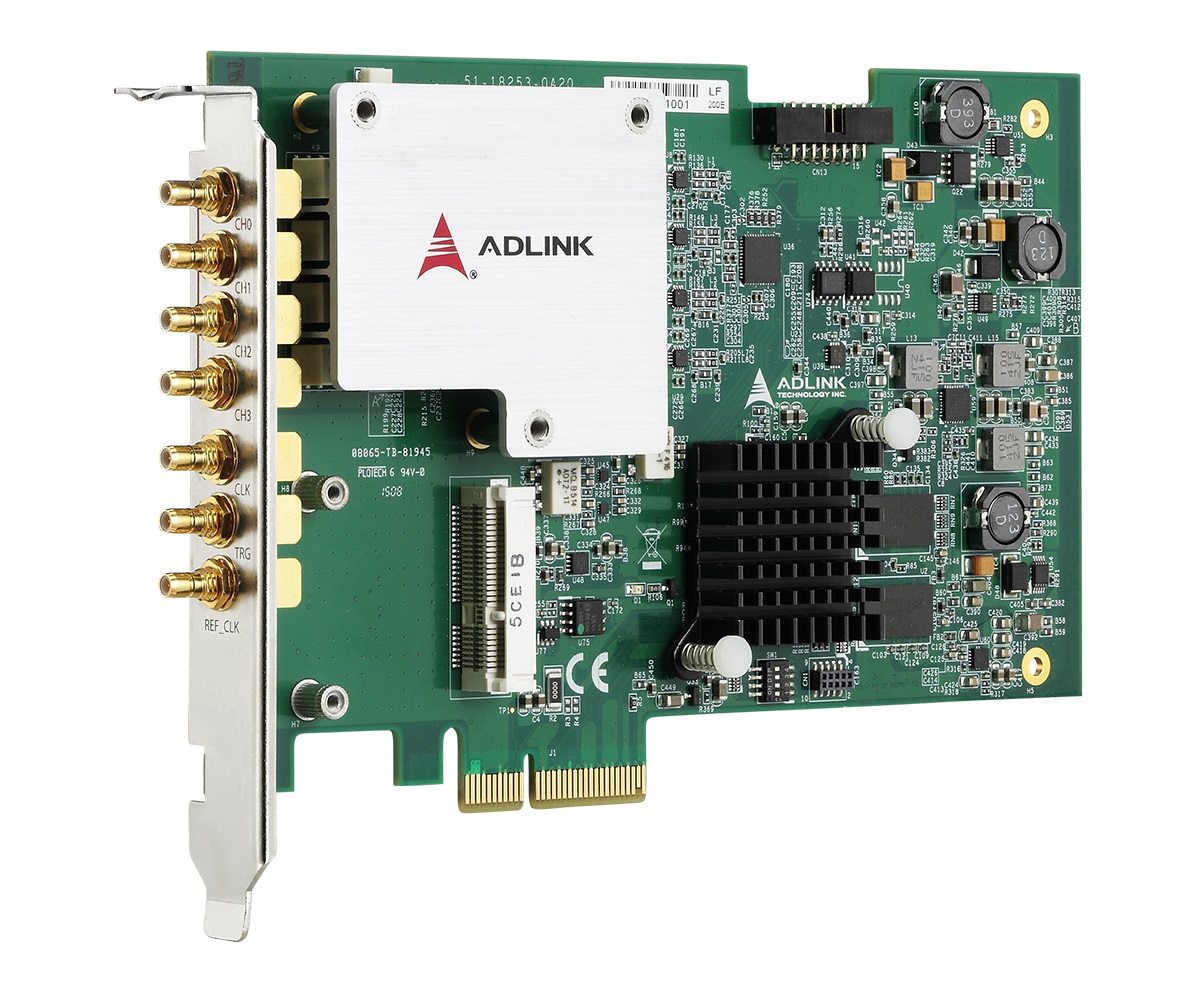
- WD-DASK - Windows driver API for PCI/PXI-9820 and PXI-98xx Digitizer
- SMB-BNC-1m - SMB to BNC cable 1m (PXI-9816/26/46)