DIN-100S-01
LOOKING FOR THE RIGHT
INDUSTRIAL SOLUTION?
Discover embedded, communication and automation solutions tailored to your application.
- CompactPCI 3U Eurocard Form Factor: Fully compliant with PICMG 2.0 R3.0 CompactPCI specifications.
- Four Onboard 8254 Programmable Timer/Counter Chips: Provides twelve 16‑bit down counters or frequency dividers.
- 10 Independent 16‑bit Counters + 2 Cascaded Counters: Ten channels can operate independently or be cascaded; two additional counters (11 and 12) are cascaded by default to form a 32‑bit timer.
- Flexible Clock Source Selection: Each counter can select from four clock sources—external clock, previous counter output, CK1, or COUT10.
- Onboard 8 MHz Clock Source: Provides a stable internal reference for timing operations.
- Programmable De‑bounce Filters: Eleven channels of glitch‑filtered external clock and interrupt inputs, with programmable de‑bounce clock up to 2 MHz.
- Dual Interrupt System: Two interrupt sources—external interrupt input and output of counter #12—allow flexible event handling.
- Digital I/O Capability: 8‑channel TTL digital inputs and 8‑channel TTL digital outputs for control and monitoring.
- Rear I/O Connectivity: 100‑pin SCSI‑II female connector for all I/O signals, including +5 V and +12 V power outputs with resettable fuses.
- Software Support: Comprehensive driver and library support for Windows and Linux, including DAQPilot, DAQBench, LabVIEW™, MATLAB®, and PCIS‑DASK.
- Operating System Compatibility: Windows 7/Vista/XP/2000/2003, Windows CE (on request), and Linux.
- Applications: Event counting, frequency generation, pulse width measurement, watchdog timer, baud‑rate generation, and industrial automation.
- Four Onboard 8254 Programmable Timer/Counter Chips: Provides twelve 16‑bit down counters or frequency dividers.
- 10 Independent 16‑bit Counters + 2 Cascaded Counters: Ten channels can operate independently or be cascaded; two additional counters (11 and 12) are cascaded by default to form a 32‑bit timer.
- Flexible Clock Source Selection: Each counter can select from four clock sources—external clock, previous counter output, CK1, or COUT10.
- Onboard 8 MHz Clock Source: Provides a stable internal reference for timing operations.
- Programmable De‑bounce Filters: Eleven channels of glitch‑filtered external clock and interrupt inputs, with programmable de‑bounce clock up to 2 MHz.
- Dual Interrupt System: Two interrupt sources—external interrupt input and output of counter #12—allow flexible event handling.
- Digital I/O Capability: 8‑channel TTL digital inputs and 8‑channel TTL digital outputs for control and monitoring.
- Rear I/O Connectivity: 100‑pin SCSI‑II female connector for all I/O signals, including +5 V and +12 V power outputs with resettable fuses.
- Software Support: Comprehensive driver and library support for Windows and Linux, including DAQPilot, DAQBench, LabVIEW™, MATLAB®, and PCIS‑DASK.
- Operating System Compatibility: Windows 7/Vista/XP/2000/2003, Windows CE (on request), and Linux.
- Applications: Event counting, frequency generation, pulse width measurement, watchdog timer, baud‑rate generation, and industrial automation.
Comprehensive Product Summary – ADLINK cPCI‑8554R CompactPCI 12‑Channel Timer/Counter Rear I/O Card
### 1. Product Overview
Product Name: cPCI‑8554R
Model: cPCI‑8554R
Series: PCI/cPCI‑8554 Series
Article Number: cPCI‑8554R
Manufacturer: ADLINK Technology Inc. (Taipei, Taiwan)
Product Type: CompactPCI 12‑Channel Timer/Counter & Digital I/O Card with Rear I/O
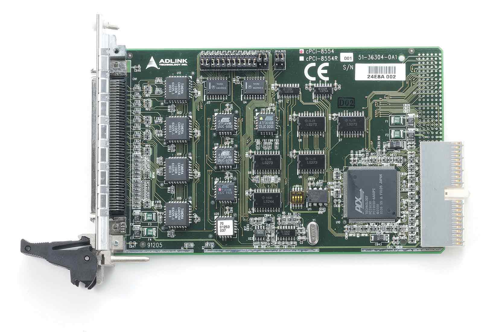
The ADLINK cPCI‑8554R is a 3U CompactPCI‑compliant multifunction counter/timer and digital I/O card designed for industrial automation, measurement, and control applications. It is part of ADLINK’s PCI/cPCI‑8554 family, which includes the PCI‑8554 (standard PCI), cPCI‑8554 (front I/O CompactPCI), and cPCI‑8554R (rear I/O CompactPCI) variants. The “R” version provides rear I/O connectivity through a 100‑pin SCSI‑II female connector, enabling clean cabling and integration in CompactPCI systems.
### 2. Key Features
- CompactPCI 3U Eurocard Form Factor: Fully compliant with PICMG 2.0 R3.0 CompactPCI specifications.
- Four Onboard 8254 Programmable Timer/Counter Chips: Provides twelve 16‑bit down counters or frequency dividers.
- 10 Independent 16‑bit Counters + 2 Cascaded Counters: Ten channels can operate independently or be cascaded; two additional counters (11 and 12) are cascaded by default to form a 32‑bit timer.
- Flexible Clock Source Selection: Each counter can select from four clock sources—external clock, previous counter output, CK1, or COUT10.
- Onboard 8 MHz Clock Source: Provides a stable internal reference for timing operations.
- Programmable De‑bounce Filters: Eleven channels of glitch‑filtered external clock and interrupt inputs, with programmable de‑bounce clock up to 2 MHz.
- Dual Interrupt System: Two interrupt sources—external interrupt input and output of counter #12—allow flexible event handling.
- Digital I/O Capability: 8‑channel TTL digital inputs and 8‑channel TTL digital outputs for control and monitoring.
- Rear I/O Connectivity: 100‑pin SCSI‑II female connector for all I/O signals, including +5 V and +12 V power outputs with resettable fuses.
- Software Support: Comprehensive driver and library support for Windows and Linux, including DAQPilot, DAQBench, LabVIEW™, MATLAB®, and PCIS‑DASK.
- Operating System Compatibility: Windows 7/Vista/XP/2000/2003, Windows CE (on request), and Linux.
- Applications: Event counting, frequency generation, pulse width measurement, watchdog timer, baud‑rate generation, and industrial automation.
### 3. Technical Specifications
Form Factor: 3U CompactPCI (PICMG 2.0 R3.0 compliant)
Dimensions: 160 mm × 100 mm (cPCI‑8554/8554R)
Weight: Approx. 200 g (typical board weight)
Bus Interface: 32‑bit, 5 V CompactPCI bus
Power Requirements: +5 V @ 350 mA (typical)
Power Output (via connector): +5 V and +12 V available, each protected by resettable fuses (0.5 A max per line)
Operating Temperature: 0 °C – 60 °C
Storage Temperature: −20 °C – 80 °C
Relative Humidity: 5 % – 95 %, non‑condensing
Connector Type: One 100‑pin SCSI‑II female (rear I/O)
Timer/Counter Subsystem:
- Number of Counters: 12 total (10 independent + 2 cascaded)
- Counter Width: 16 bits (independent), 32 bits (cascaded)
- Base Clock: 8 MHz internal or external up to 10 MHz
- Counter Device: Four Intel/NEC 82C54 programmable interval timers
- Counter Modes: 16‑bit down counter, programmable modes 0–5 (per 8254 specification)
- Maximum Input Frequency: 10 MHz
- Clock Sources per Counter: External (ECLKn), previous counter output (COUTn‑1), CK1, or COUT10
- CK1 Clock Sources: 8 MHz internal or COUT11 (programmable)
- Gate Control: Default enabled (logic high) or externally controlled via GATEn input
- Cascaded Timer: Counter #11 → #12, forming a 32‑bit timer with fixed 8 MHz base clock
Digital I/O:
- 8 × TTL Digital Inputs (DI0–DI7)
- 8 × TTL Digital Outputs (DO0–DO7)
- Logic Level: 5 V TTL compatible
- Data Transfer: Programmed I/O
De‑bounce Filter:
- Channels: 11 (10 × external clocks + 1 × external interrupt)
- Glitch Rejection: 4 × periods of de‑bounce clock
- De‑bounce Clock: Programmable up to 2 MHz
- Clock Source: COUT11 or fixed 2 MHz (software selectable)
Interrupt System:
- Interrupt Sources: 2 (external interrupt input, counter #12 output)
- Interrupt Type: Dual interrupt system, single PCI INT #A line
- Software Functions: Enable/disable, clear, and status query via driver API
### 4. Functionality
The cPCI‑8554R operates as a multifunction timing and counting module for CompactPCI systems. Each of its twelve counters can be configured independently or cascaded to form extended‑width counters. The onboard 8 MHz oscillator provides a stable timing reference, while external clock inputs allow synchronization with external events up to 10 MHz.
Operation Principles:
- Each 8254 chip provides three counters, each with clock, gate, and output signals.
- Counters #1–#10 can be configured as independent or cascaded; counters #11 and #12 are cascaded by default.
- The card supports software‑selectable clock routing, enabling complex timing chains (e.g., multi‑stage frequency division).
- The dual interrupt system allows event‑driven operation, with interrupts triggered by external signals or internal timer outputs.
- The digital I/O ports provide general‑purpose control and monitoring of external TTL devices.
Typical Use Cases:
- Event Counting: Counting pulses from sensors or encoders.
- Frequency Generation: Producing square‑wave outputs from 0.00186 Hz to 2 MHz.
- Pulse Width Measurement: Measuring signal duration using gate‑controlled counters.
- Frequency Measurement: Determining input signal frequency by counting events within a precise time window.
- Watchdog Timer: Using cascaded counters to generate periodic interrupts for system supervision.
- Industrial Automation: Timing control, process synchronization, and machine monitoring.
Compatibility:
- CompactPCI backplane (3U, 32‑bit, 5 V signaling)
- Rear I/O interface via CompactPCI J2 connector (not PXI‑compatible due to signal conflicts)
- Compatible with ADLINK terminal boards (DIN‑100S‑01) and cables (ACL‑10252‑1)
### 5. Components & Accessories
Included Items:
- cPCI‑8554R Counter/Timer & DIO Card
- ADLINK Software & Driver CD
- Software Installation Guide
- User’s Manual (PDF)
Optional Accessories:
- DIN‑100S‑01: Terminal board with one 100‑pin SCSI‑II connector and DIN‑rail mounting.
- ACL‑10252‑1: 100‑pin to dual 50‑pin cable (1 m) for legacy DIN‑502S replacement.
- Cables: Standard 100‑pin SCSI‑II shielded cables for signal breakout.
Connectors & Signals:
- 100‑pin SCSI‑II female connector carrying all counter, gate, clock, digital I/O, interrupt, and power lines.
- +5 V and +12 V outputs available for powering external circuits (protected by resettable fuses).
- Signal groups include ECLKn (external clocks), GATEn (gate inputs), COUTn (counter outputs), DI/DO lines, and E_INT (external interrupt).
### 6. Installation & Setup
System Requirements:
- CompactPCI chassis with 3U slot and 5 V signaling
- Supported OS: Windows 7/Vista/XP/2000/2003, Linux, Windows CE (optional)
- Available PCI interrupt and I/O address space (assigned automatically by BIOS)
Installation Procedure:
1. Power off the CompactPCI system and disconnect peripherals.
2. Insert the cPCI‑8554R into an available 3U CompactPCI slot.
3. Secure the card to the chassis.
4. Power on the system; the Plug‑and‑Play BIOS assigns resources automatically.
5. Install ADLINK drivers (PCIS‑DASK or DAQPilot) from the provided CD.
6. Verify installation using ADLINK’s diagnostic utilities.
Jumper Configuration:
- JP1–JP11: Enable/disable de‑bounce for ECLK1–ECLK10 and E_INT.
- JP12–JP13: Select clock source for counters #11 and #12 (default cascaded).
- JP14–JP15 (cPCI‑8554R only): Select gate voltage for counters #11 and #12 (default = Vcc).
Mounting Options:
Rear I/O connection through CompactPCI backplane; external wiring via rear transition module or terminal board.
Software Setup:
Install PCIS‑DASK or DAQPilot drivers, then configure channels and modes using AD‑Logger, DAQBench, or custom applications via C/C++, VB, or LabVIEW APIs.
### 7. Performance & Capabilities
Timing Performance:
- Internal Clock Frequency: 8 MHz
- External Clock Frequency: up to 10 MHz
- Minimum Time Resolution: 125 ns (at 8 MHz)
- Maximum Cascaded Counter Width: 160 bits (10 × 16‑bit counters cascaded)
- Cascaded 32‑bit Timer Output Range: 0.00186 Hz – 2 MHz
Digital I/O Performance:
- TTL logic levels (0 V = low, 2.4 V min = high)
- Input/Output current: ±2 mA typical
- Programmed I/O transfer mode
Interrupt Handling:
- Dual interrupt sources with software‑selectable enable/disable
- Single PCI INT #A line to host
- Interrupt latency dependent on OS and driver configuration
Efficiency & Reliability:
- Hardware de‑bounce filtering ensures accurate counting of noisy signals.
- Resettable fuses protect power outputs from overload.
- ASIC PCI controller ensures full Plug‑and‑Play compliance and automatic resource allocation.
Limitations:
- Rear I/O version (cPCI‑8554R) cannot be used in PXI chassis due to signal conflicts with PXI trigger bus.
- External clock frequency limited to 10 MHz maximum.
- De‑bounce clock limited to 2 MHz.
### 8. Standards & Compliance
- CompactPCI Compliance: PICMG 2.0 R3.0
- PCI Local Bus Specification: Revision 2.1 (32‑bit, 5 V signaling)
- Electrical Compatibility: TTL/CMOS logic levels
- Environmental Compliance: Designed for industrial temperature and humidity ranges
- Safety & EMC: Conforms to CE and FCC Class A industrial standards (per ADLINK manufacturing policy)
- Software Standards: Compatible with major DAQ frameworks (LabVIEW™, MATLAB®, DAQBench™, etc.)
- RoHS Compliance: ADLINK manufacturing processes conform to RoHS environmental directives.
### 9. Additional Information
Warranty:
- Standard 2‑year limited warranty (1 year in China).
- Covers defects in materials and workmanship from date of shipment.
- Excludes damage from misuse, improper installation, or unauthorized repair.
- Return merchandise authorization (RMA) required for service.
Support & Maintenance:
- Technical support via email: service@adlinktech.com
- Web resources: [www.adlinktech.com](http://www.adlinktech.com)
- Regional support for NuDAQ, NuIPC, and automation products.
- Firmware and driver updates available online.
- Preventive maintenance: periodic inspection of connectors and fuses recommended.
Software & Driver Updates:
- Windows Drivers: PCIS‑DASK, DAQPilot, DAQBench ActiveX, LabVIEW VIs.
- Linux Drivers: PCIS‑DASK/X shared library.
- Programming Languages Supported: C/C++, VB, Delphi, .NET, MATLAB.
- Example Applications: Frequency generation, pulse measurement, event counting, watchdog timer, and interrupt‑driven control.
Documentation:
- User’s Guide (Rev 1.02, July 31 2002)
- Software Installation Guide
- Function Reference Manuals for PCIS‑DASK and DAQPilot
- Application examples and C/C++ source code (DEMO1.C – DEMO5.C)
Manufacturer Contact:
ADLINK Technology Inc.
9F, No. 166, Jian Yi Road, Chungho City, Taipei 235, Taiwan
Tel: +886‑2‑8226‑5877 Fax: +886‑2‑8226‑5717
Email: service@adlinktech.com
### Summary
The ADLINK cPCI‑8554R is a high‑precision, multi‑channel timer/counter and digital I/O card engineered for CompactPCI systems requiring deterministic timing, event counting, and signal generation. With four 8254 timer chips, twelve counters, dual interrupt capability, and robust software support, it provides a flexible and reliable platform for industrial measurement and control. Its rear I/O design simplifies system integration in CompactPCI environments, while programmable de‑bounce filters and multiple clock sources ensure accurate operation even in noisy industrial conditions. The cPCI‑8554R exemplifies ADLINK’s commitment to modular, standards‑compliant, and software‑integrated data acquisition solutions for automation and embedded control applications.

### 1. Product Overview
Product Name: cPCI‑8554R
Model: cPCI‑8554R
Series: PCI/cPCI‑8554 Series
Article Number: cPCI‑8554R
Manufacturer: ADLINK Technology Inc. (Taipei, Taiwan)
Product Type: CompactPCI 12‑Channel Timer/Counter & Digital I/O Card with Rear I/O
The ADLINK cPCI‑8554R is a 3U CompactPCI‑compliant multifunction counter/timer and digital I/O card designed for industrial automation, measurement, and control applications. It is part of ADLINK’s PCI/cPCI‑8554 family, which includes the PCI‑8554 (standard PCI), cPCI‑8554 (front I/O CompactPCI), and cPCI‑8554R (rear I/O CompactPCI) variants. The “R” version provides rear I/O connectivity through a 100‑pin SCSI‑II female connector, enabling clean cabling and integration in CompactPCI systems.
### 2. Key Features
- CompactPCI 3U Eurocard Form Factor: Fully compliant with PICMG 2.0 R3.0 CompactPCI specifications.
- Four Onboard 8254 Programmable Timer/Counter Chips: Provides twelve 16‑bit down counters or frequency dividers.
- 10 Independent 16‑bit Counters + 2 Cascaded Counters: Ten channels can operate independently or be cascaded; two additional counters (11 and 12) are cascaded by default to form a 32‑bit timer.
- Flexible Clock Source Selection: Each counter can select from four clock sources—external clock, previous counter output, CK1, or COUT10.
- Onboard 8 MHz Clock Source: Provides a stable internal reference for timing operations.
- Programmable De‑bounce Filters: Eleven channels of glitch‑filtered external clock and interrupt inputs, with programmable de‑bounce clock up to 2 MHz.
- Dual Interrupt System: Two interrupt sources—external interrupt input and output of counter #12—allow flexible event handling.
- Digital I/O Capability: 8‑channel TTL digital inputs and 8‑channel TTL digital outputs for control and monitoring.
- Rear I/O Connectivity: 100‑pin SCSI‑II female connector for all I/O signals, including +5 V and +12 V power outputs with resettable fuses.
- Software Support: Comprehensive driver and library support for Windows and Linux, including DAQPilot, DAQBench, LabVIEW™, MATLAB®, and PCIS‑DASK.
- Operating System Compatibility: Windows 7/Vista/XP/2000/2003, Windows CE (on request), and Linux.
- Applications: Event counting, frequency generation, pulse width measurement, watchdog timer, baud‑rate generation, and industrial automation.
### 3. Technical Specifications
Form Factor: 3U CompactPCI (PICMG 2.0 R3.0 compliant)
Dimensions: 160 mm × 100 mm (cPCI‑8554/8554R)
Weight: Approx. 200 g (typical board weight)
Bus Interface: 32‑bit, 5 V CompactPCI bus
Power Requirements: +5 V @ 350 mA (typical)
Power Output (via connector): +5 V and +12 V available, each protected by resettable fuses (0.5 A max per line)
Operating Temperature: 0 °C – 60 °C
Storage Temperature: −20 °C – 80 °C
Relative Humidity: 5 % – 95 %, non‑condensing
Connector Type: One 100‑pin SCSI‑II female (rear I/O)
Timer/Counter Subsystem:
- Number of Counters: 12 total (10 independent + 2 cascaded)
- Counter Width: 16 bits (independent), 32 bits (cascaded)
- Base Clock: 8 MHz internal or external up to 10 MHz
- Counter Device: Four Intel/NEC 82C54 programmable interval timers
- Counter Modes: 16‑bit down counter, programmable modes 0–5 (per 8254 specification)
- Maximum Input Frequency: 10 MHz
- Clock Sources per Counter: External (ECLKn), previous counter output (COUTn‑1), CK1, or COUT10
- CK1 Clock Sources: 8 MHz internal or COUT11 (programmable)
- Gate Control: Default enabled (logic high) or externally controlled via GATEn input
- Cascaded Timer: Counter #11 → #12, forming a 32‑bit timer with fixed 8 MHz base clock
Digital I/O:
- 8 × TTL Digital Inputs (DI0–DI7)
- 8 × TTL Digital Outputs (DO0–DO7)
- Logic Level: 5 V TTL compatible
- Data Transfer: Programmed I/O
De‑bounce Filter:
- Channels: 11 (10 × external clocks + 1 × external interrupt)
- Glitch Rejection: 4 × periods of de‑bounce clock
- De‑bounce Clock: Programmable up to 2 MHz
- Clock Source: COUT11 or fixed 2 MHz (software selectable)
Interrupt System:
- Interrupt Sources: 2 (external interrupt input, counter #12 output)
- Interrupt Type: Dual interrupt system, single PCI INT #A line
- Software Functions: Enable/disable, clear, and status query via driver API
### 4. Functionality
The cPCI‑8554R operates as a multifunction timing and counting module for CompactPCI systems. Each of its twelve counters can be configured independently or cascaded to form extended‑width counters. The onboard 8 MHz oscillator provides a stable timing reference, while external clock inputs allow synchronization with external events up to 10 MHz.
Operation Principles:
- Each 8254 chip provides three counters, each with clock, gate, and output signals.
- Counters #1–#10 can be configured as independent or cascaded; counters #11 and #12 are cascaded by default.
- The card supports software‑selectable clock routing, enabling complex timing chains (e.g., multi‑stage frequency division).
- The dual interrupt system allows event‑driven operation, with interrupts triggered by external signals or internal timer outputs.
- The digital I/O ports provide general‑purpose control and monitoring of external TTL devices.
Typical Use Cases:
- Event Counting: Counting pulses from sensors or encoders.
- Frequency Generation: Producing square‑wave outputs from 0.00186 Hz to 2 MHz.
- Pulse Width Measurement: Measuring signal duration using gate‑controlled counters.
- Frequency Measurement: Determining input signal frequency by counting events within a precise time window.
- Watchdog Timer: Using cascaded counters to generate periodic interrupts for system supervision.
- Industrial Automation: Timing control, process synchronization, and machine monitoring.
Compatibility:
- CompactPCI backplane (3U, 32‑bit, 5 V signaling)
- Rear I/O interface via CompactPCI J2 connector (not PXI‑compatible due to signal conflicts)
- Compatible with ADLINK terminal boards (DIN‑100S‑01) and cables (ACL‑10252‑1)
### 5. Components & Accessories
Included Items:
- cPCI‑8554R Counter/Timer & DIO Card
- ADLINK Software & Driver CD
- Software Installation Guide
- User’s Manual (PDF)
Optional Accessories:
- DIN‑100S‑01: Terminal board with one 100‑pin SCSI‑II connector and DIN‑rail mounting.
- ACL‑10252‑1: 100‑pin to dual 50‑pin cable (1 m) for legacy DIN‑502S replacement.
- Cables: Standard 100‑pin SCSI‑II shielded cables for signal breakout.
Connectors & Signals:
- 100‑pin SCSI‑II female connector carrying all counter, gate, clock, digital I/O, interrupt, and power lines.
- +5 V and +12 V outputs available for powering external circuits (protected by resettable fuses).
- Signal groups include ECLKn (external clocks), GATEn (gate inputs), COUTn (counter outputs), DI/DO lines, and E_INT (external interrupt).
### 6. Installation & Setup
System Requirements:
- CompactPCI chassis with 3U slot and 5 V signaling
- Supported OS: Windows 7/Vista/XP/2000/2003, Linux, Windows CE (optional)
- Available PCI interrupt and I/O address space (assigned automatically by BIOS)
Installation Procedure:
1. Power off the CompactPCI system and disconnect peripherals.
2. Insert the cPCI‑8554R into an available 3U CompactPCI slot.
3. Secure the card to the chassis.
4. Power on the system; the Plug‑and‑Play BIOS assigns resources automatically.
5. Install ADLINK drivers (PCIS‑DASK or DAQPilot) from the provided CD.
6. Verify installation using ADLINK’s diagnostic utilities.
Jumper Configuration:
- JP1–JP11: Enable/disable de‑bounce for ECLK1–ECLK10 and E_INT.
- JP12–JP13: Select clock source for counters #11 and #12 (default cascaded).
- JP14–JP15 (cPCI‑8554R only): Select gate voltage for counters #11 and #12 (default = Vcc).
Mounting Options:
Rear I/O connection through CompactPCI backplane; external wiring via rear transition module or terminal board.
Software Setup:
Install PCIS‑DASK or DAQPilot drivers, then configure channels and modes using AD‑Logger, DAQBench, or custom applications via C/C++, VB, or LabVIEW APIs.
### 7. Performance & Capabilities
Timing Performance:
- Internal Clock Frequency: 8 MHz
- External Clock Frequency: up to 10 MHz
- Minimum Time Resolution: 125 ns (at 8 MHz)
- Maximum Cascaded Counter Width: 160 bits (10 × 16‑bit counters cascaded)
- Cascaded 32‑bit Timer Output Range: 0.00186 Hz – 2 MHz
Digital I/O Performance:
- TTL logic levels (0 V = low, 2.4 V min = high)
- Input/Output current: ±2 mA typical
- Programmed I/O transfer mode
Interrupt Handling:
- Dual interrupt sources with software‑selectable enable/disable
- Single PCI INT #A line to host
- Interrupt latency dependent on OS and driver configuration
Efficiency & Reliability:
- Hardware de‑bounce filtering ensures accurate counting of noisy signals.
- Resettable fuses protect power outputs from overload.
- ASIC PCI controller ensures full Plug‑and‑Play compliance and automatic resource allocation.
Limitations:
- Rear I/O version (cPCI‑8554R) cannot be used in PXI chassis due to signal conflicts with PXI trigger bus.
- External clock frequency limited to 10 MHz maximum.
- De‑bounce clock limited to 2 MHz.
### 8. Standards & Compliance
- CompactPCI Compliance: PICMG 2.0 R3.0
- PCI Local Bus Specification: Revision 2.1 (32‑bit, 5 V signaling)
- Electrical Compatibility: TTL/CMOS logic levels
- Environmental Compliance: Designed for industrial temperature and humidity ranges
- Safety & EMC: Conforms to CE and FCC Class A industrial standards (per ADLINK manufacturing policy)
- Software Standards: Compatible with major DAQ frameworks (LabVIEW™, MATLAB®, DAQBench™, etc.)
- RoHS Compliance: ADLINK manufacturing processes conform to RoHS environmental directives.
### 9. Additional Information
Warranty:
- Standard 2‑year limited warranty (1 year in China).
- Covers defects in materials and workmanship from date of shipment.
- Excludes damage from misuse, improper installation, or unauthorized repair.
- Return merchandise authorization (RMA) required for service.
Support & Maintenance:
- Technical support via email: service@adlinktech.com
- Web resources: [www.adlinktech.com](http://www.adlinktech.com)
- Regional support for NuDAQ, NuIPC, and automation products.
- Firmware and driver updates available online.
- Preventive maintenance: periodic inspection of connectors and fuses recommended.
Software & Driver Updates:
- Windows Drivers: PCIS‑DASK, DAQPilot, DAQBench ActiveX, LabVIEW VIs.
- Linux Drivers: PCIS‑DASK/X shared library.
- Programming Languages Supported: C/C++, VB, Delphi, .NET, MATLAB.
- Example Applications: Frequency generation, pulse measurement, event counting, watchdog timer, and interrupt‑driven control.
Documentation:
- User’s Guide (Rev 1.02, July 31 2002)
- Software Installation Guide
- Function Reference Manuals for PCIS‑DASK and DAQPilot
- Application examples and C/C++ source code (DEMO1.C – DEMO5.C)
Manufacturer Contact:
ADLINK Technology Inc.
9F, No. 166, Jian Yi Road, Chungho City, Taipei 235, Taiwan
Tel: +886‑2‑8226‑5877 Fax: +886‑2‑8226‑5717
Email: service@adlinktech.com
### Summary
The ADLINK cPCI‑8554R is a high‑precision, multi‑channel timer/counter and digital I/O card engineered for CompactPCI systems requiring deterministic timing, event counting, and signal generation. With four 8254 timer chips, twelve counters, dual interrupt capability, and robust software support, it provides a flexible and reliable platform for industrial measurement and control. Its rear I/O design simplifies system integration in CompactPCI environments, while programmable de‑bounce filters and multiple clock sources ensure accurate operation even in noisy industrial conditions. The cPCI‑8554R exemplifies ADLINK’s commitment to modular, standards‑compliant, and software‑integrated data acquisition solutions for automation and embedded control applications.
-
cPCI-8554_Datasheet_en_1.pdf
PDF Catalog
-
cPCI-8554+R_Manual_4_en.pdf
Manual
-
P8554 Manual.PDF
Manual
- DIN-100S-01 - 100pin SCSI-II termination board DIN rail w/o cable
- DIN-502S - 2*50pin SCSI-II termination board DIN rail