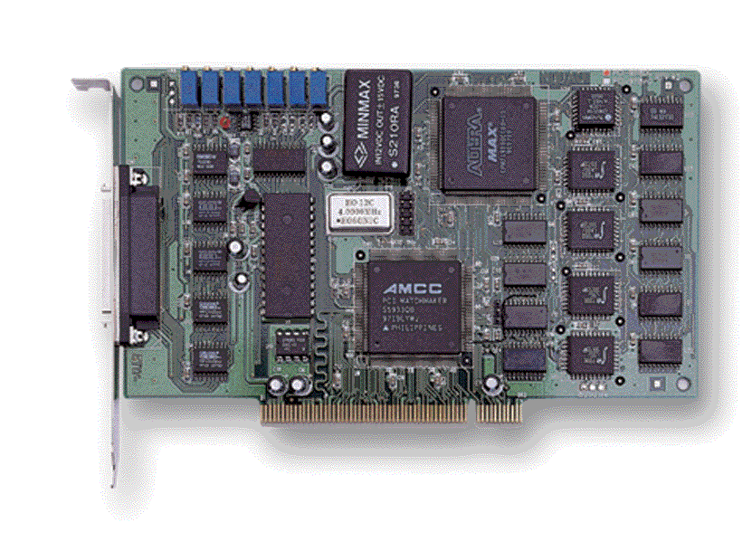
DIN-50S-01
LOOKING FOR THE RIGHT
INDUSTRIAL SOLUTION?
Discover embedded, communication and automation solutions tailored to your application.
- High-Speed Analog Input:
12-bit resolution with up to 333 kS/s sampling rate (DG/HG models).
16 single-ended or 8 differential analog input channels.
- Analog Output:
Two 12-bit monolithic multiplying DAC channels (±10 V output range).
- FIFO Buffer:
1K-sample onboard A/D FIFO memory for high-speed data streaming.
- Channel-Gain Queue:
256-entry hardware queue allowing per-channel gain and range configuration for sequential sampling.
- Programmable Gain:
x1, x2, x4, x8 for DG/HR models; software-selectable bipolar/unipolar ranges.
- Triggering and Sampling Modes:
- Software, programmable pacer, or external pulse trigger.
- Pre-trigger, post-trigger, and about-trigger acquisition modes.
- Burst mode and burst mode with sample-and-hold (SSH) emulation.
- Digital I/O:
4 TTL-compatible digital inputs and 4 digital outputs.
- Timer/Counter:
82C54 programmable counter with 32-bit pacer timer (4 MHz base clock).
- Interface:
32-bit PCI bus, plug-and-play configuration, 50-pin SCSI-II type connector.
- Software Support:
Comprehensive driver suite for Windows and DOS, including LabVIEW®, HP-VEE™, DASYLab™, InTouch™, InControl™, ISaGRAF™, and OPC server support.
- Compact Design:
Half-size PCI card suitable for embedded and industrial PCs.
12-bit resolution with up to 333 kS/s sampling rate (DG/HG models).
16 single-ended or 8 differential analog input channels.
- Analog Output:
Two 12-bit monolithic multiplying DAC channels (±10 V output range).
- FIFO Buffer:
1K-sample onboard A/D FIFO memory for high-speed data streaming.
- Channel-Gain Queue:
256-entry hardware queue allowing per-channel gain and range configuration for sequential sampling.
- Programmable Gain:
x1, x2, x4, x8 for DG/HR models; software-selectable bipolar/unipolar ranges.
- Triggering and Sampling Modes:
- Software, programmable pacer, or external pulse trigger.
- Pre-trigger, post-trigger, and about-trigger acquisition modes.
- Burst mode and burst mode with sample-and-hold (SSH) emulation.
- Digital I/O:
4 TTL-compatible digital inputs and 4 digital outputs.
- Timer/Counter:
82C54 programmable counter with 32-bit pacer timer (4 MHz base clock).
- Interface:
32-bit PCI bus, plug-and-play configuration, 50-pin SCSI-II type connector.
- Software Support:
Comprehensive driver suite for Windows and DOS, including LabVIEW®, HP-VEE™, DASYLab™, InTouch™, InControl™, ISaGRAF™, and OPC server support.
- Compact Design:
Half-size PCI card suitable for embedded and industrial PCs.
Comprehensive Product Summary – ADLINK NuDAQ PCI-9118DG
### 1. Product Overview
Product Name: PCI-9118DG
Model: PCI-9118DG
Series: NuDAQ PCI-9118 Series (DG/HG/HR variants)
Article Number: 91-12255-002
Manufacturer: ADLINK Technology Inc.
Product Type: PCI-Bus Advanced Data Acquisition (DAQ) Card
Form Factor: Half-size PCI card (173 mm × 102 mm)
End-of-Life Notice: EOL No. 20051121-001, published November 21, 2005
The ADLINK PCI-9118DG is a multifunction, high-performance data acquisition card designed for industrial, laboratory, and process control applications. It belongs to the NuDAQ PCI-9118 family, which includes the DG (12-bit, low gain), HG (12-bit, high gain), and HR (16-bit, high-resolution) models. The PCI-9118DG variant provides 12-bit analog input resolution, 333 kS/s sampling rate, 16 single-ended or 8 differential analog input channels, dual 12-bit analog outputs, digital I/O, and a programmable counter/timer.
### 2. Key Features
- High-Speed Analog Input:
12-bit resolution with up to 333 kS/s sampling rate (DG/HG models).
16 single-ended or 8 differential analog input channels.
- Analog Output:
Two 12-bit monolithic multiplying DAC channels (±10 V output range).
- FIFO Buffer:
1K-sample onboard A/D FIFO memory for high-speed data streaming.
- Channel-Gain Queue:
256-entry hardware queue allowing per-channel gain and range configuration for sequential sampling.
- Programmable Gain:
x1, x2, x4, x8 for DG/HR models; software-selectable bipolar/unipolar ranges.
- Triggering and Sampling Modes:
- Software, programmable pacer, or external pulse trigger.
- Pre-trigger, post-trigger, and about-trigger acquisition modes.
- Burst mode and burst mode with sample-and-hold (SSH) emulation.
- Digital I/O:
4 TTL-compatible digital inputs and 4 digital outputs.
- Timer/Counter:
82C54 programmable counter with 32-bit pacer timer (4 MHz base clock).
- Interface:
32-bit PCI bus, plug-and-play configuration, 50-pin SCSI-II type connector.
- Software Support:
Comprehensive driver suite for Windows and DOS, including LabVIEW®, HP-VEE™, DASYLab™, InTouch™, InControl™, ISaGRAF™, and OPC server support.
- Compact Design:
Half-size PCI card suitable for embedded and industrial PCs.
### 3. Technical Specifications
Analog Input (A/D):
- Converter: Burr-Brown ADS7800 or equivalent
- Channels: 16 single-ended or 8 differential
- Resolution: 12-bit
- Sampling Rate: Up to 333 kS/s
- FIFO Buffer: 1024 samples
- Channel/Gain Queue: 256 entries
- Input Range (software-selectable):
- Bipolar: ±5 V, ±2.5 V, ±1.25 V, ±0.625 V
- Unipolar: 0–10 V, 0–5 V, 0–2.5 V, 0–1.25 V
- Input Impedance: 10 GΩ || 6 pF
- Accuracy: ±0.01% FSR ±1 LSB (typical)
- Overvoltage Protection: ±70 V peak-to-peak
- Trigger Modes: Pre-, Post-, About-trigger
- Data Transfer: Programmed I/O, Interrupt, or DMA (bus mastering)
Analog Output (D/A):
- Channels: 2
- Resolution: 12-bit
- Output Range: ±10 V (bipolar)
- Converter: Burr-Brown DAC2813 or equivalent
- Settling Time: 4.5 µs typical, 6 µs max
- Linearity: ±0.5 LSB max, ±0.25 LSB typical
- Output Drive: ±5 mA minimum
- Modes: Double-buffered or transparent
Digital I/O:
- Channels: 4 inputs, 4 outputs (TTL/DTL compatible)
- Input Voltage:
- Low ≤ 0.8 V, High ≥ 2.0 V
- Output Voltage:
- Low ≤ 0.5 V @ 8 mA, High ≥ 2.7 V @ 400 µA
Timer/Counter:
- Device: Intel/NEC 82C54
- Configuration: 3 × 16-bit counters (Counter 1 & 2 cascaded for pacer)
- Base Clock: 4 MHz
- Pacer Rate: 0.0012 Hz to 333 kHz
General:
- Connector: 50-pin SCSI-II D-type female
- Dimensions: 173 mm (L) × 102 mm (H)
- Operating Temperature: 0°C to 60°C
- Storage Temperature: -20°C to 80°C
- Humidity: 5–95% non-condensing
- Power Consumption:
+5 V @ 450 mA, +12 V @ 200 mA, -12 V @ 50 mA
### 4. Functionality
Operation Principle:
The PCI-9118DG performs analog-to-digital conversion triggered by software, internal pacer, or external signals. It supports continuous, burst, and triggered acquisition modes. The onboard FIFO and DMA bus mastering enable high-speed, low-latency data transfer to system memory.
Use Cases:
- Industrial process monitoring and control
- Laboratory data logging and waveform analysis
- Energy management and automation systems
- Product testing and quality assurance
- Event counting and frequency measurement
- Signal generation and control applications
Compatibility:
- PCI 2.1 compliant 32-bit bus interface
- Supported OS: DOS, Windows 95/98/NT/2000
- Supported software: LabVIEW®, HP-VEE™, DASYLab™, InTouch™, ISaGRAF™, InControl™, OPC
### 5. Components & Accessories
Included Items:
- PCI-9118DG data acquisition card
- ADLINK software CD (drivers, utilities, manuals)
- Software Installation Guide
- User’s Guide
Connector (CN1, 50-pin SCSI-II):
- Analog Inputs: AI0–AI15 (single-ended) or AIH0–AIH7 / AIL0–AIL7 (differential)
- Analog Outputs: DAC0, DAC1
- Digital I/O: DI0–DI3, DO0–DO3
- Trigger and Timer: EXTTRG, TGIN, TGOUT, SSHO
- Power and Grounds: ±15 V, A.GND, D.GND, VCC
Optional Accessories:
- Shielded cable assemblies
- Terminal boards for signal breakout
- Calibration utilities and software packages
### 6. Installation & Setup
System Requirements:
- Available 32-bit PCI slot
- Compatible PC with Windows 95/98/NT/2000 or DOS
- Administrative privileges for driver installation
Installation Steps:
1. Power off the PC and disconnect peripherals.
2. Insert the PCI-9118DG into an available PCI slot.
3. Secure the card and reconnect system power.
4. Windows Plug-and-Play automatically detects the card.
5. Install drivers from the ADLINK CD following the Software Installation Guide.
Configuration:
- Automatic IRQ and I/O address assignment via BIOS.
- Manual jumper settings for analog input mode (single-ended/differential) and D/A reference voltage.
Signal Connection:
- Use CN1 for all analog, digital, and timing signals.
- Observe grounding and shielding best practices to minimize noise.
### 7. Performance & Capabilities
Analog Input Performance:
- Maximum Throughput: 333 kS/s (aggregate)
- Resolution: 12 bits
- Accuracy: ±0.01% FSR ±1 LSB
- Input Impedance: 10 GΩ || 6 pF
- Overvoltage Protection: ±70 V
Analog Output Performance:
- Resolution: 12 bits
- Settling Time: 4.5 µs typical
- Output Range: ±10 V
- Drive Capability: ±5 mA
Digital I/O:
- TTL-compatible, 4 input and 4 output lines
- Suitable for control, status monitoring, and event signaling
Timer/Counter:
- 32-bit pacer timer with 4 MHz base clock
- Programmable rate generation from 0.0012 Hz to 333 kHz
Limitations:
- 12-bit resolution limits fine precision compared to 16-bit HR model
- Single-ended mode susceptible to ground noise if improperly configured
### 8. Standards & Compliance
- Bus Interface: PCI Local Bus Specification Rev. 2.1 compliant
- Electrical Safety: Designed for low-voltage DC operation within PC chassis
- EMC Compliance: Meets industrial EMI/EMC standards (when installed in compliant systems)
- Software Standards:
- OPC, DDE, ActiveX, and LabVIEW driver compatibility
- IEC 1131-3 SoftPLC support via ISaGRAF driver
### 9. Additional Information
Calibration:
- Onboard variable resistors (VR1–VR7) for A/D and D/A calibration:
- VR1/VR3: D/A full-scale adjustment
- VR2/VR4: D/A offset adjustment
- VR5–VR7: A/D full-scale and offset calibration
- Calibration utility (9118util.exe) included for guided software calibration.
- Recommended recalibration interval:
- 3 months (industrial environments)
- 6–12 months (laboratory conditions)
Software Utilities:
- 9118util.exe provides:
- System configuration
- Calibration routines
- Functional testing (DI/DO, A/D polling, DMA, burst, and trigger tests)
Warranty:
- 1-year limited warranty from date of purchase
- Covers defects in materials and workmanship
- Excludes damage from misuse, modification, or operation beyond specifications
Support & Maintenance:
- Technical support via ADLINK website and authorized distributors
- Firmware and driver updates available on ADLINK’s support portal
- Replacement recommendation: DAQ-2214 for full analog I/O functionality
End-of-Life Notice:
- EOL Publication Date: November 21, 2005
- Last Order Date: December 15, 2005
- Replacement Product: DAQ-2214 (for analog I/O applications)
### Summary
The ADLINK PCI-9118DG is a robust, multifunction PCI data acquisition card engineered for high-speed, high-accuracy analog and digital signal processing. With 12-bit resolution, 333 kS/s throughput, dual analog outputs, and integrated digital I/O, it provides a versatile platform for industrial automation, laboratory measurement, and control systems. Its flexible triggering, DMA support, and comprehensive software ecosystem make it suitable for both real-time and batch data acquisition tasks. Despite its EOL status, the PCI-9118DG remains a benchmark in PCI-based DAQ design, offering a balance of performance, reliability, and software integration.

### 1. Product Overview
Product Name: PCI-9118DG
Model: PCI-9118DG
Series: NuDAQ PCI-9118 Series (DG/HG/HR variants)
Article Number: 91-12255-002
Manufacturer: ADLINK Technology Inc.
Product Type: PCI-Bus Advanced Data Acquisition (DAQ) Card
Form Factor: Half-size PCI card (173 mm × 102 mm)
End-of-Life Notice: EOL No. 20051121-001, published November 21, 2005
The ADLINK PCI-9118DG is a multifunction, high-performance data acquisition card designed for industrial, laboratory, and process control applications. It belongs to the NuDAQ PCI-9118 family, which includes the DG (12-bit, low gain), HG (12-bit, high gain), and HR (16-bit, high-resolution) models. The PCI-9118DG variant provides 12-bit analog input resolution, 333 kS/s sampling rate, 16 single-ended or 8 differential analog input channels, dual 12-bit analog outputs, digital I/O, and a programmable counter/timer.
### 2. Key Features
- High-Speed Analog Input:
12-bit resolution with up to 333 kS/s sampling rate (DG/HG models).
16 single-ended or 8 differential analog input channels.
- Analog Output:
Two 12-bit monolithic multiplying DAC channels (±10 V output range).
- FIFO Buffer:
1K-sample onboard A/D FIFO memory for high-speed data streaming.
- Channel-Gain Queue:
256-entry hardware queue allowing per-channel gain and range configuration for sequential sampling.
- Programmable Gain:
x1, x2, x4, x8 for DG/HR models; software-selectable bipolar/unipolar ranges.
- Triggering and Sampling Modes:
- Software, programmable pacer, or external pulse trigger.
- Pre-trigger, post-trigger, and about-trigger acquisition modes.
- Burst mode and burst mode with sample-and-hold (SSH) emulation.
- Digital I/O:
4 TTL-compatible digital inputs and 4 digital outputs.
- Timer/Counter:
82C54 programmable counter with 32-bit pacer timer (4 MHz base clock).
- Interface:
32-bit PCI bus, plug-and-play configuration, 50-pin SCSI-II type connector.
- Software Support:
Comprehensive driver suite for Windows and DOS, including LabVIEW®, HP-VEE™, DASYLab™, InTouch™, InControl™, ISaGRAF™, and OPC server support.
- Compact Design:
Half-size PCI card suitable for embedded and industrial PCs.
### 3. Technical Specifications
Analog Input (A/D):
- Converter: Burr-Brown ADS7800 or equivalent
- Channels: 16 single-ended or 8 differential
- Resolution: 12-bit
- Sampling Rate: Up to 333 kS/s
- FIFO Buffer: 1024 samples
- Channel/Gain Queue: 256 entries
- Input Range (software-selectable):
- Bipolar: ±5 V, ±2.5 V, ±1.25 V, ±0.625 V
- Unipolar: 0–10 V, 0–5 V, 0–2.5 V, 0–1.25 V
- Input Impedance: 10 GΩ || 6 pF
- Accuracy: ±0.01% FSR ±1 LSB (typical)
- Overvoltage Protection: ±70 V peak-to-peak
- Trigger Modes: Pre-, Post-, About-trigger
- Data Transfer: Programmed I/O, Interrupt, or DMA (bus mastering)
Analog Output (D/A):
- Channels: 2
- Resolution: 12-bit
- Output Range: ±10 V (bipolar)
- Converter: Burr-Brown DAC2813 or equivalent
- Settling Time: 4.5 µs typical, 6 µs max
- Linearity: ±0.5 LSB max, ±0.25 LSB typical
- Output Drive: ±5 mA minimum
- Modes: Double-buffered or transparent
Digital I/O:
- Channels: 4 inputs, 4 outputs (TTL/DTL compatible)
- Input Voltage:
- Low ≤ 0.8 V, High ≥ 2.0 V
- Output Voltage:
- Low ≤ 0.5 V @ 8 mA, High ≥ 2.7 V @ 400 µA
Timer/Counter:
- Device: Intel/NEC 82C54
- Configuration: 3 × 16-bit counters (Counter 1 & 2 cascaded for pacer)
- Base Clock: 4 MHz
- Pacer Rate: 0.0012 Hz to 333 kHz
General:
- Connector: 50-pin SCSI-II D-type female
- Dimensions: 173 mm (L) × 102 mm (H)
- Operating Temperature: 0°C to 60°C
- Storage Temperature: -20°C to 80°C
- Humidity: 5–95% non-condensing
- Power Consumption:
+5 V @ 450 mA, +12 V @ 200 mA, -12 V @ 50 mA
### 4. Functionality
Operation Principle:
The PCI-9118DG performs analog-to-digital conversion triggered by software, internal pacer, or external signals. It supports continuous, burst, and triggered acquisition modes. The onboard FIFO and DMA bus mastering enable high-speed, low-latency data transfer to system memory.
Use Cases:
- Industrial process monitoring and control
- Laboratory data logging and waveform analysis
- Energy management and automation systems
- Product testing and quality assurance
- Event counting and frequency measurement
- Signal generation and control applications
Compatibility:
- PCI 2.1 compliant 32-bit bus interface
- Supported OS: DOS, Windows 95/98/NT/2000
- Supported software: LabVIEW®, HP-VEE™, DASYLab™, InTouch™, ISaGRAF™, InControl™, OPC
### 5. Components & Accessories
Included Items:
- PCI-9118DG data acquisition card
- ADLINK software CD (drivers, utilities, manuals)
- Software Installation Guide
- User’s Guide
Connector (CN1, 50-pin SCSI-II):
- Analog Inputs: AI0–AI15 (single-ended) or AIH0–AIH7 / AIL0–AIL7 (differential)
- Analog Outputs: DAC0, DAC1
- Digital I/O: DI0–DI3, DO0–DO3
- Trigger and Timer: EXTTRG, TGIN, TGOUT, SSHO
- Power and Grounds: ±15 V, A.GND, D.GND, VCC
Optional Accessories:
- Shielded cable assemblies
- Terminal boards for signal breakout
- Calibration utilities and software packages
### 6. Installation & Setup
System Requirements:
- Available 32-bit PCI slot
- Compatible PC with Windows 95/98/NT/2000 or DOS
- Administrative privileges for driver installation
Installation Steps:
1. Power off the PC and disconnect peripherals.
2. Insert the PCI-9118DG into an available PCI slot.
3. Secure the card and reconnect system power.
4. Windows Plug-and-Play automatically detects the card.
5. Install drivers from the ADLINK CD following the Software Installation Guide.
Configuration:
- Automatic IRQ and I/O address assignment via BIOS.
- Manual jumper settings for analog input mode (single-ended/differential) and D/A reference voltage.
Signal Connection:
- Use CN1 for all analog, digital, and timing signals.
- Observe grounding and shielding best practices to minimize noise.
### 7. Performance & Capabilities
Analog Input Performance:
- Maximum Throughput: 333 kS/s (aggregate)
- Resolution: 12 bits
- Accuracy: ±0.01% FSR ±1 LSB
- Input Impedance: 10 GΩ || 6 pF
- Overvoltage Protection: ±70 V
Analog Output Performance:
- Resolution: 12 bits
- Settling Time: 4.5 µs typical
- Output Range: ±10 V
- Drive Capability: ±5 mA
Digital I/O:
- TTL-compatible, 4 input and 4 output lines
- Suitable for control, status monitoring, and event signaling
Timer/Counter:
- 32-bit pacer timer with 4 MHz base clock
- Programmable rate generation from 0.0012 Hz to 333 kHz
Limitations:
- 12-bit resolution limits fine precision compared to 16-bit HR model
- Single-ended mode susceptible to ground noise if improperly configured
### 8. Standards & Compliance
- Bus Interface: PCI Local Bus Specification Rev. 2.1 compliant
- Electrical Safety: Designed for low-voltage DC operation within PC chassis
- EMC Compliance: Meets industrial EMI/EMC standards (when installed in compliant systems)
- Software Standards:
- OPC, DDE, ActiveX, and LabVIEW driver compatibility
- IEC 1131-3 SoftPLC support via ISaGRAF driver
### 9. Additional Information
Calibration:
- Onboard variable resistors (VR1–VR7) for A/D and D/A calibration:
- VR1/VR3: D/A full-scale adjustment
- VR2/VR4: D/A offset adjustment
- VR5–VR7: A/D full-scale and offset calibration
- Calibration utility (9118util.exe) included for guided software calibration.
- Recommended recalibration interval:
- 3 months (industrial environments)
- 6–12 months (laboratory conditions)
Software Utilities:
- 9118util.exe provides:
- System configuration
- Calibration routines
- Functional testing (DI/DO, A/D polling, DMA, burst, and trigger tests)
Warranty:
- 1-year limited warranty from date of purchase
- Covers defects in materials and workmanship
- Excludes damage from misuse, modification, or operation beyond specifications
Support & Maintenance:
- Technical support via ADLINK website and authorized distributors
- Firmware and driver updates available on ADLINK’s support portal
- Replacement recommendation: DAQ-2214 for full analog I/O functionality
End-of-Life Notice:
- EOL Publication Date: November 21, 2005
- Last Order Date: December 15, 2005
- Replacement Product: DAQ-2214 (for analog I/O applications)
### Summary
The ADLINK PCI-9118DG is a robust, multifunction PCI data acquisition card engineered for high-speed, high-accuracy analog and digital signal processing. With 12-bit resolution, 333 kS/s throughput, dual analog outputs, and integrated digital I/O, it provides a versatile platform for industrial automation, laboratory measurement, and control systems. Its flexible triggering, DMA support, and comprehensive software ecosystem make it suitable for both real-time and batch data acquisition tasks. Despite its EOL status, the PCI-9118DG remains a benchmark in PCI-based DAQ design, offering a balance of performance, reliability, and software integration.
-
PCI-9118 Manual.PDF
Manual
- DIN-50S-01 - 50pin SCSI-II termination board w/o cable DIN rail
- ACL-10250-1 - 50pin SCSI-II cable 1m
- ACL-10250-2 - 50pin SCSI-II cable 2m
- ACL-10250-4 - 50pin SCSI-II cable 4m