WD-DASK
LOOKING FOR THE RIGHT
INDUSTRIAL SOLUTION?
Discover embedded, communication and automation solutions tailored to your application.
- PCI Express Specification Compliance: PCI Express Rev. 1.1, Gen 1 x4 interface
- High‑Resolution ADC: 24‑bit delta‑sigma analog‑to‑digital converters for superior accuracy
- Simultaneous Sampling: Eight channels sampled concurrently for phase‑coherent measurements
- Sampling Rate: Up to 192 kS/s per channel, adjustable in fine increments
- Input Range: Software‑selectable ±10 V or ±1 V
- Input Coupling: AC or DC, software‑selectable; AC coupling cutoff frequency 0.5 Hz
- IEPE Sensor Support: 4 mA excitation current per channel, 24 V compliance for accelerometers and microphones
- Auto‑Calibration: Onboard reference circuit with EEPROM‑stored calibration constants
- Triggering Options: Software, external digital, analog, and SSI (System Synchronization Interface) triggers
- Synchronization: Multi‑module synchronization via SSI bus for timebase and trigger sharing
- Data Transfer: Scatter‑gather DMA for high‑speed, continuous data streaming
- Onboard Memory: 512 MB shared buffer for data acquisition
- Software Compatibility: LabVIEW®, MATLAB®, Visual Studio®, and ADLINK DSA‑DASK SDK
- Operating Systems: Windows XP/7/8 (x86/x64)
- Certifications: CE, FCC Class A, RoHS, and WEEE compliant
- High‑Resolution ADC: 24‑bit delta‑sigma analog‑to‑digital converters for superior accuracy
- Simultaneous Sampling: Eight channels sampled concurrently for phase‑coherent measurements
- Sampling Rate: Up to 192 kS/s per channel, adjustable in fine increments
- Input Range: Software‑selectable ±10 V or ±1 V
- Input Coupling: AC or DC, software‑selectable; AC coupling cutoff frequency 0.5 Hz
- IEPE Sensor Support: 4 mA excitation current per channel, 24 V compliance for accelerometers and microphones
- Auto‑Calibration: Onboard reference circuit with EEPROM‑stored calibration constants
- Triggering Options: Software, external digital, analog, and SSI (System Synchronization Interface) triggers
- Synchronization: Multi‑module synchronization via SSI bus for timebase and trigger sharing
- Data Transfer: Scatter‑gather DMA for high‑speed, continuous data streaming
- Onboard Memory: 512 MB shared buffer for data acquisition
- Software Compatibility: LabVIEW®, MATLAB®, Visual Studio®, and ADLINK DSA‑DASK SDK
- Operating Systems: Windows XP/7/8 (x86/x64)
- Certifications: CE, FCC Class A, RoHS, and WEEE compliant
Comprehensive Product Summary – ADLINK PCIe‑9529 Dynamic Signal Acquisition Module
### 1. Product Overview
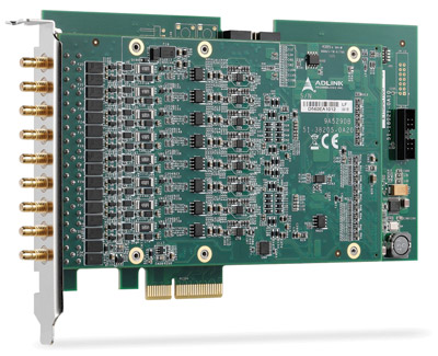
Product Name: PCIe‑9529
Model: PCIe‑9529
Series: High‑Resolution Dynamic Signal Acquisition Modules
Article Number: 50‑11255‑1000
Manufacturer: ADLINK Technology, Inc.
Product Type: PCI Express (PCIe) 8‑Channel, 24‑Bit, 192 kS/s Dynamic Signal Acquisition Module
The ADLINK PCIe‑9529 is a high‑performance, high‑density analog input card designed for precision dynamic signal acquisition. It provides eight simultaneously sampled 24‑bit channels with a maximum sampling rate of 192 kS/s per channel. The module is optimized for vibration, acoustic, and structural monitoring applications, offering exceptional dynamic range, low noise, and integrated IEPE sensor support.
### 2. Key Features
- PCI Express Specification Compliance: PCI Express Rev. 1.1, Gen 1 x4 interface
- High‑Resolution ADC: 24‑bit delta‑sigma analog‑to‑digital converters for superior accuracy
- Simultaneous Sampling: Eight channels sampled concurrently for phase‑coherent measurements
- Sampling Rate: Up to 192 kS/s per channel, adjustable in fine increments
- Input Range: Software‑selectable ±10 V or ±1 V
- Input Coupling: AC or DC, software‑selectable; AC coupling cutoff frequency 0.5 Hz
- IEPE Sensor Support: 4 mA excitation current per channel, 24 V compliance for accelerometers and microphones
- Auto‑Calibration: Onboard reference circuit with EEPROM‑stored calibration constants
- Triggering Options: Software, external digital, analog, and SSI (System Synchronization Interface) triggers
- Synchronization: Multi‑module synchronization via SSI bus for timebase and trigger sharing
- Data Transfer: Scatter‑gather DMA for high‑speed, continuous data streaming
- Onboard Memory: 512 MB shared buffer for data acquisition
- Software Compatibility: LabVIEW®, MATLAB®, Visual Studio®, and ADLINK DSA‑DASK SDK
- Operating Systems: Windows XP/7/8 (x86/x64)
- Certifications: CE, FCC Class A, RoHS, and WEEE compliant
### 3. Technical Specifications
Analog Input
- Channels: 8 simultaneous, differential or pseudo‑differential
- Resolution: 24 bits
- ADC Type: Delta‑sigma
- Sampling Rate: 8 kS/s to 192 kS/s
- 8–54 kS/s: 192 µS/s increments
- 54–108 kS/s: 576 µS/s increments
- 108–192 kS/s: 768 µS/s increments
- Input Range: ±10 V or ±1 V
- Input Impedance:
- Differential: 1 MΩ to system ground
- Pseudo‑differential: 1 MΩ (positive terminal), 50 Ω (negative terminal to ground)
- Coupling: AC/DC, software‑selectable
- AC Cutoff Frequency: 0.5 Hz
- IEPE Excitation: 4 mA per channel, 24 V compliance
- Overvoltage Protection:
- Differential: ±42.4 V
- Pseudo‑differential: +42.4 V (positive), ±2.5 V (negative terminal unprotected)
- Offset Error: ±1 mV max
- Gain Error: ±0.1% of full‑scale range
- Crosstalk: < –100 dB
- THD: < –104 dB
- Dynamic Range: 100–107 dBFS (depending on sample rate)
- SNR: up to 104 dBc
- SFDR: up to 105 dBc
- Flatness: ±0.06 to ±0.1 dB (20 Hz–42 kHz)
- Common Mode Rejection Ratio (CMRR): 65 dB (±1 V), 80 dB (±10 V)
Timebase and Clocking
- Internal Timebase: 10 MHz synthesizer (< ±25 ppm accuracy)
- External Timebase: SSI bus input
- Onboard Oscillator: 80 MHz
- Delay Trigger Timebase: PCIe clock (125 MHz)
- Reference Voltage: +5.000 V, < 5 ppm/°C drift, 15‑minute warm‑up
Triggering
- Sources: Software, external digital, analog, SSI
- Modes: Post‑trigger, delay‑trigger, re‑trigger
- External Digital Trigger:
- Connector: Front‑panel SMB
- Compatibility: 3.3 V TTL, 5 V tolerant
- Thresholds: VIH ≥ 2.0 V, VIL ≤ 0.8 V
- Pulse Width: ≥ 20 ns
- Polarity: Rising or falling edge selectable
- Analog Trigger: Programmable level (24‑bit resolution) on any channel
- SSI Synchronization: SSI_TIMEBASE, SSI_SYNC_START, SSI_AD_TRIG
Physical and Environmental
- Dimensions: 160 mm (W) × 100 mm (H) (6.24" × 3.9")
- Weight: Approx. 0.5 kg (typical)
- Bus Interface: PCI Express Gen 1 x4
- Operating Temperature: 0°C to 55°C (32°F to 131°F)
- Storage Temperature: –20°C to 80°C (–4°F to 176°F)
- Humidity: 10%–90%, non‑condensing
- Power Consumption:
- +3.3 V rail: 584 mA (standby), 630 mA (full load)
- +12 V rail: 904 mA (standby), 1160 mA (full load)
Connectors
- Analog Inputs: 8 × SMB
- External Digital Trigger: 1 × SMB
- SSI Bus: CN4 connector (8‑line bus)
### 4. Functionality
The PCIe‑9529 operates as a high‑precision dynamic signal digitizer. Each of its eight channels employs a 24‑bit delta‑sigma ADC with simultaneous sampling, ensuring phase alignment across all inputs. The module supports both differential and pseudo‑differential configurations, allowing flexible interfacing with grounded or floating signal sources.
Use Cases and Applications:
- Structural health monitoring
- Noise, vibration, and harshness (NVH) testing
- Machine condition monitoring
- Acoustic and audio analysis
- Phased array data acquisition
- Laboratory and industrial signal measurement
Compatibility:
- Compatible with standard PCI Express x4 slots
- Supported by ADLINK’s DSA‑DASK driver library and SDKs for LabVIEW, MATLAB, and Visual Studio environments
### 5. Components & Accessories
Included Items:
- PCIe‑9529 module
- ADLINK All‑in‑One software CD (drivers, SDKs, documentation)
- Quick Start Guide
Optional Accessories:
- SMB‑to‑BNC cables for analog input connections
- SSI synchronization cables for multi‑module setups
- Mounting brackets and anti‑static handling accessories
Connectors:
- 8 × SMB connectors for analog input channels
- 1 × SMB connector for external digital trigger input
- CN4 connector for SSI synchronization bus
### 6. Installation & Setup
Requirements:
- Available PCI Express x4 slot
- Compatible host system running Windows XP/7/8 (x86/x64)
- Administrator privileges for driver installation
Installation Steps:
1. Power off the host computer and remove the cover.
2. Insert the PCIe‑9529 into an available PCIe x4 slot.
3. Secure the bracket with the retaining screw.
4. Replace the computer cover and power on the system.
5. Install ADLINK DSA‑DASK drivers and verify device recognition.
Setup Notes:
- Handle the module using an anti‑static wrist strap and mat.
- Allow a 15‑minute warm‑up period for calibration stability.
- Use the DSA Utility or SDK for configuration of sampling rate, coupling, and trigger modes.
### 7. Performance & Capabilities
Sampling and Conversion:
- 24‑bit resolution ensures high dynamic range and low quantization noise.
- Sigma‑delta ADC architecture provides superior linearity and noise shaping.
- Simultaneous sampling across all channels eliminates phase skew.
Data Throughput:
- Maximum data rate: 3.072 MB/s (192 kS/s × 8 channels × 3 bytes/sample)
- Scatter‑gather DMA enables continuous streaming without CPU overhead.
- Onboard FIFO buffers (1,024 samples per channel) prevent data loss during transfer.
Efficiency and Limitations:
- Optimized for dynamic signal acquisition rather than static DC measurement.
- AC coupling cutoff at 0.5 Hz limits ultra‑low‑frequency response.
- Pseudo‑differential negative terminal unprotected beyond ±2.5 V.
Synchronization:
- SSI bus allows multiple PCIe‑9529 modules to share a common timebase and trigger.
- Master/slave configuration ensures coherent sampling across systems.
### 8. Standards & Compliance
Electrical and Mechanical Standards:
- PCI Express Base Specification Rev. 1.1 compliant
- PXI Express mechanical form factor compatibility (for PXIe‑9529 variant)
Regulatory Compliance:
- CE (Electromagnetic Compatibility)
- FCC Class A (Electromagnetic Interference)
- RoHS (Restriction of Hazardous Substances)
- WEEE (Waste Electrical and Electronic Equipment Directive)
Environmental Responsibility:
ADLINK adheres to global environmental standards, ensuring that all materials and manufacturing processes minimize ecological impact. Products are designed for safe recycling and disposal in accordance with local regulations.
### 9. Additional Information
Calibration and Maintenance:
- Factory‑calibrated prior to shipment; constants stored in EEPROM (Bank 0).
- Auto‑calibration function available for user‑initiated recalibration (stored in Bank 1).
- Recommended warm‑up: 20 minutes before calibration.
- No external reference required for auto‑calibration.
Warranty and Support:
- Standard ADLINK limited warranty (contact regional office for terms).
- Global technical support available via email and phone.
- Service centers located in Taiwan, USA, China, Japan, Korea, Singapore, Germany, France, India, and Israel.
Software and Updates:
- DSA‑DASK driver package includes DLLs and APIs for Windows.
- SDKs: DAQPilot for LabVIEW, MATLAB toolbox adapter, and Visual Studio libraries.
- Regular firmware and driver updates available from ADLINK’s website.
Safety and Handling:
- Operate only within specified environmental limits.
- Avoid exposure to moisture, heat, or static discharge.
- Service only by qualified personnel.
- Lithium backup battery (if present) must be replaced with identical type to prevent explosion risk.
### Summary
The ADLINK PCIe‑9529 is a precision 8‑channel, 24‑bit, 192 kS/s dynamic signal acquisition module engineered for high‑fidelity measurement of vibration, acoustic, and structural signals. Its combination of simultaneous sampling, wide dynamic range, and integrated IEPE sensor support makes it ideal for demanding test and measurement environments. With robust synchronization, flexible triggering, and comprehensive software support, the PCIe‑9529 delivers laboratory‑grade performance in a compact PCIe form factor suitable for industrial and research applications.
Manufacturer Contact:
ADLINK Technology, Inc.
9F, No.166 Jian Yi Road, Zhonghe District, New Taipei City 235, Taiwan
Tel: +886‑2‑8226‑5877 | Email: service@adlinktech.com
Website: [www.adlinktech.com](https://www.adlinktech.com)

### 1. Product Overview
Product Name: PCIe‑9529
Model: PCIe‑9529
Series: High‑Resolution Dynamic Signal Acquisition Modules
Article Number: 50‑11255‑1000
Manufacturer: ADLINK Technology, Inc.
Product Type: PCI Express (PCIe) 8‑Channel, 24‑Bit, 192 kS/s Dynamic Signal Acquisition Module
The ADLINK PCIe‑9529 is a high‑performance, high‑density analog input card designed for precision dynamic signal acquisition. It provides eight simultaneously sampled 24‑bit channels with a maximum sampling rate of 192 kS/s per channel. The module is optimized for vibration, acoustic, and structural monitoring applications, offering exceptional dynamic range, low noise, and integrated IEPE sensor support.
### 2. Key Features
- PCI Express Specification Compliance: PCI Express Rev. 1.1, Gen 1 x4 interface
- High‑Resolution ADC: 24‑bit delta‑sigma analog‑to‑digital converters for superior accuracy
- Simultaneous Sampling: Eight channels sampled concurrently for phase‑coherent measurements
- Sampling Rate: Up to 192 kS/s per channel, adjustable in fine increments
- Input Range: Software‑selectable ±10 V or ±1 V
- Input Coupling: AC or DC, software‑selectable; AC coupling cutoff frequency 0.5 Hz
- IEPE Sensor Support: 4 mA excitation current per channel, 24 V compliance for accelerometers and microphones
- Auto‑Calibration: Onboard reference circuit with EEPROM‑stored calibration constants
- Triggering Options: Software, external digital, analog, and SSI (System Synchronization Interface) triggers
- Synchronization: Multi‑module synchronization via SSI bus for timebase and trigger sharing
- Data Transfer: Scatter‑gather DMA for high‑speed, continuous data streaming
- Onboard Memory: 512 MB shared buffer for data acquisition
- Software Compatibility: LabVIEW®, MATLAB®, Visual Studio®, and ADLINK DSA‑DASK SDK
- Operating Systems: Windows XP/7/8 (x86/x64)
- Certifications: CE, FCC Class A, RoHS, and WEEE compliant
### 3. Technical Specifications
Analog Input
- Channels: 8 simultaneous, differential or pseudo‑differential
- Resolution: 24 bits
- ADC Type: Delta‑sigma
- Sampling Rate: 8 kS/s to 192 kS/s
- 8–54 kS/s: 192 µS/s increments
- 54–108 kS/s: 576 µS/s increments
- 108–192 kS/s: 768 µS/s increments
- Input Range: ±10 V or ±1 V
- Input Impedance:
- Differential: 1 MΩ to system ground
- Pseudo‑differential: 1 MΩ (positive terminal), 50 Ω (negative terminal to ground)
- Coupling: AC/DC, software‑selectable
- AC Cutoff Frequency: 0.5 Hz
- IEPE Excitation: 4 mA per channel, 24 V compliance
- Overvoltage Protection:
- Differential: ±42.4 V
- Pseudo‑differential: +42.4 V (positive), ±2.5 V (negative terminal unprotected)
- Offset Error: ±1 mV max
- Gain Error: ±0.1% of full‑scale range
- Crosstalk: < –100 dB
- THD: < –104 dB
- Dynamic Range: 100–107 dBFS (depending on sample rate)
- SNR: up to 104 dBc
- SFDR: up to 105 dBc
- Flatness: ±0.06 to ±0.1 dB (20 Hz–42 kHz)
- Common Mode Rejection Ratio (CMRR): 65 dB (±1 V), 80 dB (±10 V)
Timebase and Clocking
- Internal Timebase: 10 MHz synthesizer (< ±25 ppm accuracy)
- External Timebase: SSI bus input
- Onboard Oscillator: 80 MHz
- Delay Trigger Timebase: PCIe clock (125 MHz)
- Reference Voltage: +5.000 V, < 5 ppm/°C drift, 15‑minute warm‑up
Triggering
- Sources: Software, external digital, analog, SSI
- Modes: Post‑trigger, delay‑trigger, re‑trigger
- External Digital Trigger:
- Connector: Front‑panel SMB
- Compatibility: 3.3 V TTL, 5 V tolerant
- Thresholds: VIH ≥ 2.0 V, VIL ≤ 0.8 V
- Pulse Width: ≥ 20 ns
- Polarity: Rising or falling edge selectable
- Analog Trigger: Programmable level (24‑bit resolution) on any channel
- SSI Synchronization: SSI_TIMEBASE, SSI_SYNC_START, SSI_AD_TRIG
Physical and Environmental
- Dimensions: 160 mm (W) × 100 mm (H) (6.24" × 3.9")
- Weight: Approx. 0.5 kg (typical)
- Bus Interface: PCI Express Gen 1 x4
- Operating Temperature: 0°C to 55°C (32°F to 131°F)
- Storage Temperature: –20°C to 80°C (–4°F to 176°F)
- Humidity: 10%–90%, non‑condensing
- Power Consumption:
- +3.3 V rail: 584 mA (standby), 630 mA (full load)
- +12 V rail: 904 mA (standby), 1160 mA (full load)
Connectors
- Analog Inputs: 8 × SMB
- External Digital Trigger: 1 × SMB
- SSI Bus: CN4 connector (8‑line bus)
### 4. Functionality
The PCIe‑9529 operates as a high‑precision dynamic signal digitizer. Each of its eight channels employs a 24‑bit delta‑sigma ADC with simultaneous sampling, ensuring phase alignment across all inputs. The module supports both differential and pseudo‑differential configurations, allowing flexible interfacing with grounded or floating signal sources.
Use Cases and Applications:
- Structural health monitoring
- Noise, vibration, and harshness (NVH) testing
- Machine condition monitoring
- Acoustic and audio analysis
- Phased array data acquisition
- Laboratory and industrial signal measurement
Compatibility:
- Compatible with standard PCI Express x4 slots
- Supported by ADLINK’s DSA‑DASK driver library and SDKs for LabVIEW, MATLAB, and Visual Studio environments
### 5. Components & Accessories
Included Items:
- PCIe‑9529 module
- ADLINK All‑in‑One software CD (drivers, SDKs, documentation)
- Quick Start Guide
Optional Accessories:
- SMB‑to‑BNC cables for analog input connections
- SSI synchronization cables for multi‑module setups
- Mounting brackets and anti‑static handling accessories
Connectors:
- 8 × SMB connectors for analog input channels
- 1 × SMB connector for external digital trigger input
- CN4 connector for SSI synchronization bus
### 6. Installation & Setup
Requirements:
- Available PCI Express x4 slot
- Compatible host system running Windows XP/7/8 (x86/x64)
- Administrator privileges for driver installation
Installation Steps:
1. Power off the host computer and remove the cover.
2. Insert the PCIe‑9529 into an available PCIe x4 slot.
3. Secure the bracket with the retaining screw.
4. Replace the computer cover and power on the system.
5. Install ADLINK DSA‑DASK drivers and verify device recognition.
Setup Notes:
- Handle the module using an anti‑static wrist strap and mat.
- Allow a 15‑minute warm‑up period for calibration stability.
- Use the DSA Utility or SDK for configuration of sampling rate, coupling, and trigger modes.
### 7. Performance & Capabilities
Sampling and Conversion:
- 24‑bit resolution ensures high dynamic range and low quantization noise.
- Sigma‑delta ADC architecture provides superior linearity and noise shaping.
- Simultaneous sampling across all channels eliminates phase skew.
Data Throughput:
- Maximum data rate: 3.072 MB/s (192 kS/s × 8 channels × 3 bytes/sample)
- Scatter‑gather DMA enables continuous streaming without CPU overhead.
- Onboard FIFO buffers (1,024 samples per channel) prevent data loss during transfer.
Efficiency and Limitations:
- Optimized for dynamic signal acquisition rather than static DC measurement.
- AC coupling cutoff at 0.5 Hz limits ultra‑low‑frequency response.
- Pseudo‑differential negative terminal unprotected beyond ±2.5 V.
Synchronization:
- SSI bus allows multiple PCIe‑9529 modules to share a common timebase and trigger.
- Master/slave configuration ensures coherent sampling across systems.
### 8. Standards & Compliance
Electrical and Mechanical Standards:
- PCI Express Base Specification Rev. 1.1 compliant
- PXI Express mechanical form factor compatibility (for PXIe‑9529 variant)
Regulatory Compliance:
- CE (Electromagnetic Compatibility)
- FCC Class A (Electromagnetic Interference)
- RoHS (Restriction of Hazardous Substances)
- WEEE (Waste Electrical and Electronic Equipment Directive)
Environmental Responsibility:
ADLINK adheres to global environmental standards, ensuring that all materials and manufacturing processes minimize ecological impact. Products are designed for safe recycling and disposal in accordance with local regulations.
### 9. Additional Information
Calibration and Maintenance:
- Factory‑calibrated prior to shipment; constants stored in EEPROM (Bank 0).
- Auto‑calibration function available for user‑initiated recalibration (stored in Bank 1).
- Recommended warm‑up: 20 minutes before calibration.
- No external reference required for auto‑calibration.
Warranty and Support:
- Standard ADLINK limited warranty (contact regional office for terms).
- Global technical support available via email and phone.
- Service centers located in Taiwan, USA, China, Japan, Korea, Singapore, Germany, France, India, and Israel.
Software and Updates:
- DSA‑DASK driver package includes DLLs and APIs for Windows.
- SDKs: DAQPilot for LabVIEW, MATLAB toolbox adapter, and Visual Studio libraries.
- Regular firmware and driver updates available from ADLINK’s website.
Safety and Handling:
- Operate only within specified environmental limits.
- Avoid exposure to moisture, heat, or static discharge.
- Service only by qualified personnel.
- Lithium backup battery (if present) must be replaced with identical type to prevent explosion risk.
### Summary
The ADLINK PCIe‑9529 is a precision 8‑channel, 24‑bit, 192 kS/s dynamic signal acquisition module engineered for high‑fidelity measurement of vibration, acoustic, and structural signals. Its combination of simultaneous sampling, wide dynamic range, and integrated IEPE sensor support makes it ideal for demanding test and measurement environments. With robust synchronization, flexible triggering, and comprehensive software support, the PCIe‑9529 delivers laboratory‑grade performance in a compact PCIe form factor suitable for industrial and research applications.
Manufacturer Contact:
ADLINK Technology, Inc.
9F, No.166 Jian Yi Road, Zhonghe District, New Taipei City 235, Taiwan
Tel: +886‑2‑8226‑5877 | Email: service@adlinktech.com
Website: [www.adlinktech.com](https://www.adlinktech.com)
-
PXIe-9529_datasheet_20131030.pdf
PDF Catalog

- WD-DASK - Windows driver API for PCI/PXI-9820 and PXI-98xx Digitizer
- SMB-BNC-1m - SMB to BNC cable 1m (PXI-9816/26/46)