WD-DASK
LOOKING FOR THE RIGHT
INDUSTRIAL SOLUTION?
Discover embedded, communication and automation solutions tailored to your application.
- High-Speed Sampling: Up to 80 MS/s per channel with true simultaneous sampling across four analog inputs.
- High Resolution: 12-bit analog-to-digital conversion for accurate signal representation.
- Wide Bandwidth: 40 MHz analog input bandwidth suitable for high-frequency signal capture.
- Large Onboard Memory: 1 GB shared acquisition memory enables long-duration recording at maximum sampling rates.
- Programmable Input Ranges: ±0.5 V, ±1 V, ±5 V, and ±10 V ranges selectable via software.
- Selectable Input Impedance: 50 Ω or 1 MΩ input impedance, software-configurable for flexible signal interfacing.
- Digital Filtering: FPGA-based 10 MHz or 20 MHz digital low-pass filters for noise reduction and signal conditioning.
- PLL Synchronization (PCIe-9814P only): Integrated PLL module allows precise synchronization with external reference clocks for multi-card or system-level timing alignment.
- Triggering Flexibility: Supports software, analog, external digital, and SSI (System Synchronization Interface) triggers with multiple trigger modes (pre-, post-, delay-, and middle-trigger).
- Scatter-Gather DMA: High-speed data streaming to host memory with minimal CPU overhead, supporting large continuous or segmented data transfers.
- Synchronous Digital Inputs (SDI): Three digital input lines sampled synchronously with analog channels for mixed-signal acquisition.
- Auto-Calibration: Fully automated onboard calibration with EEPROM-stored constants for long-term accuracy.
- Software Support: Compatible with Windows 7/8 (x86/x64) and Linux; drivers and SDKs available for LabVIEW, MATLAB, C/C++, Visual Basic, and Visual Studio.NET.
- Environmental Compliance: RoHS and WEEE compliant, CE and FCC Class A certified.
- High Resolution: 12-bit analog-to-digital conversion for accurate signal representation.
- Wide Bandwidth: 40 MHz analog input bandwidth suitable for high-frequency signal capture.
- Large Onboard Memory: 1 GB shared acquisition memory enables long-duration recording at maximum sampling rates.
- Programmable Input Ranges: ±0.5 V, ±1 V, ±5 V, and ±10 V ranges selectable via software.
- Selectable Input Impedance: 50 Ω or 1 MΩ input impedance, software-configurable for flexible signal interfacing.
- Digital Filtering: FPGA-based 10 MHz or 20 MHz digital low-pass filters for noise reduction and signal conditioning.
- PLL Synchronization (PCIe-9814P only): Integrated PLL module allows precise synchronization with external reference clocks for multi-card or system-level timing alignment.
- Triggering Flexibility: Supports software, analog, external digital, and SSI (System Synchronization Interface) triggers with multiple trigger modes (pre-, post-, delay-, and middle-trigger).
- Scatter-Gather DMA: High-speed data streaming to host memory with minimal CPU overhead, supporting large continuous or segmented data transfers.
- Synchronous Digital Inputs (SDI): Three digital input lines sampled synchronously with analog channels for mixed-signal acquisition.
- Auto-Calibration: Fully automated onboard calibration with EEPROM-stored constants for long-term accuracy.
- Software Support: Compatible with Windows 7/8 (x86/x64) and Linux; drivers and SDKs available for LabVIEW, MATLAB, C/C++, Visual Basic, and Visual Studio.NET.
- Environmental Compliance: RoHS and WEEE compliant, CE and FCC Class A certified.
Comprehensive Product Summary: ADLINK PCIe-9814P 4-Channel 12-Bit 80 MS/s PCI Express Digitizer
### 1. Product Overview
Product Name: PCIe-9814P
Model: PCIe-9814P
Series: PCIe-9814 Series High-Speed Digitizers
Article Number: PCIe-9814P
Manufacturer: ADLINK Technology, Inc.
Product Type: PCI Express x4 Analog-to-Digital (AD) Data Acquisition Card with PLL Synchronization Module
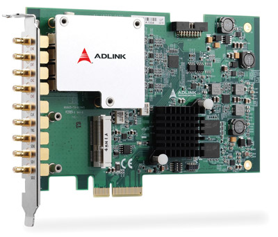
The ADLINK PCIe-9814P is a high-performance PCI Express digitizer designed for precise, high-speed analog signal acquisition. It features four simultaneous analog input channels, each capable of sampling at up to 80 mega-samples per second (MS/s) with 12-bit resolution. The card integrates a phase-locked loop (PLL) module for precise synchronization, 1 GB of onboard memory for extended data capture, and a flexible input configuration supporting multiple voltage ranges and impedance settings.
### 2. Key Features
- High-Speed Sampling: Up to 80 MS/s per channel with true simultaneous sampling across four analog inputs.
- High Resolution: 12-bit analog-to-digital conversion for accurate signal representation.
- Wide Bandwidth: 40 MHz analog input bandwidth suitable for high-frequency signal capture.
- Large Onboard Memory: 1 GB shared acquisition memory enables long-duration recording at maximum sampling rates.
- Programmable Input Ranges: ±0.5 V, ±1 V, ±5 V, and ±10 V ranges selectable via software.
- Selectable Input Impedance: 50 Ω or 1 MΩ input impedance, software-configurable for flexible signal interfacing.
- Digital Filtering: FPGA-based 10 MHz or 20 MHz digital low-pass filters for noise reduction and signal conditioning.
- PLL Synchronization (PCIe-9814P only): Integrated PLL module allows precise synchronization with external reference clocks for multi-card or system-level timing alignment.
- Triggering Flexibility: Supports software, analog, external digital, and SSI (System Synchronization Interface) triggers with multiple trigger modes (pre-, post-, delay-, and middle-trigger).
- Scatter-Gather DMA: High-speed data streaming to host memory with minimal CPU overhead, supporting large continuous or segmented data transfers.
- Synchronous Digital Inputs (SDI): Three digital input lines sampled synchronously with analog channels for mixed-signal acquisition.
- Auto-Calibration: Fully automated onboard calibration with EEPROM-stored constants for long-term accuracy.
- Software Support: Compatible with Windows 7/8 (x86/x64) and Linux; drivers and SDKs available for LabVIEW, MATLAB, C/C++, Visual Basic, and Visual Studio.NET.
- Environmental Compliance: RoHS and WEEE compliant, CE and FCC Class A certified.
### 3. Technical Specifications
Analog Input
- Channels: 4 single-ended
- Connector Type: SMB (Snap-on)
- Input Coupling: DC
- Input Impedance: 50 Ω or 1 MΩ (software selectable)
- Input Voltage Ranges: ±0.5 V, ±1 V, ±5 V, ±10 V
- Bandwidth (-3 dB): 40 MHz
- ADC Resolution: 12 bits
- Overvoltage Protection:
- ±30 V @ 1 MΩ (±5 V, ±10 V ranges)
- ±10 V @ 1 MΩ (±0.5 V, ±1 V ranges)
- ±10 V sine wave / 7 Vrms @ 50 Ω (all ranges)
- Offset Error: ±0.5 mV (±0.5 V, ±1 V), ±4 mV (±5 V), ±10 mV (±10 V)
- Gain Error: ±1% (50 Ω all ranges), ±0.5% (1 MΩ ±0.5 V, ±1 V, ±5 V), ±1% (1 MΩ ±10 V)
- Crosstalk: -80 dB (±0.5 V), -90 dB (±1 V, ±5 V, ±10 V)
- System Noise (RMS): 150 µV (±0.5 V), 300 µV (±1 V), 1.5 mV (±5 V), 2.5 mV (±10 V)
Spectral Performance (10 MHz, -1 dBFS input)
- SNR: 64–65 dB
- THD: -74 dB (filter off), -93 dB (filter on)
- SFDR: 72–78 dB depending on impedance and filter configuration
Trigger System
- Sources: Software, external digital, analog (CH0–CH3), SSI
- Modes: Post-, Pre-, Delay-, Middle-trigger, Re-trigger
- External Trigger Input:
- Connector: SMB
- Logic Level: 3.3 V TTL (5 V tolerant)
- Thresholds: VIH = 2.0 V, VIL = 0.8 V
- Max Input Range: -0.5 V to +5.5 V
- Polarity: Rising or falling edge
- Minimum Pulse Width: 20 ns
Timebase and Clocking
- Internal Clock: 1.22 kHz to 80 MHz
- External Clock Input: 20 MHz to 80 MHz (1–5 Vpp)
- External Reference Clock (PCIe-9814P only): 10 MHz via SDI0 (3.3–5 V TTL)
- Timebase Accuracy: ±25 ppm
- PLL Synchronization: Supported on PCIe-9814P
Data Storage and Transfer
- Onboard Memory: 1 GB shared among channels
- Data Transfer: Scatter-Gather DMA for continuous streaming
- Reference Voltages: +1.8 V, +0.9 V, +0.45 V (3 ppm/°C drift)
Physical and Environmental
- Dimensions: 167.64 mm (W) × 106.68 mm (H) (6.53” × 4.16”)
- Weight: Approx. 200 g (typical)
- Operating Temperature: 0°C to 50°C
- Storage Temperature: -20°C to 80°C
- Humidity: 10%–90% non-condensing
- Power Consumption:
- +3.3 V: 20 mA (standby/full load)
- +12 V: 655 mA (standby), 715 mA (full load)
- Total Power: ~8.65 W (PCIe-9814P)
Bus Interface
- PCI Express Gen 1 x4 (compatible with x4/x8/x16 slots)
### 4. Functionality
The PCIe-9814P digitizer converts analog signals into high-resolution digital data for analysis, monitoring, or control applications. Each of the four channels operates simultaneously, ensuring zero inter-channel phase delay. The onboard FPGA manages digital filtering, triggering, and DMA data streaming.
Use Cases and Applications:
- Power system monitoring and energy management (partial discharge, power line analysis)
- Non-destructive testing (NDT) and ultrasonic inspection
- Radar and LiDAR signal acquisition
- Scientific instrumentation and transient signal capture
- Mixed-signal testing with synchronous digital inputs
Compatibility:
- Operating Systems: Windows 7/8 (x86/x64), Linux
- Software Environments: LabVIEW, MATLAB, C/C++, Visual Basic, Visual Studio.NET
- Driver Packages: WD-DASK, DAQPilot, DAQLite
### 5. Components & Accessories
Included Items:
- PCIe-9814P digitizer card
- ADLINK All-in-One software CD (drivers, SDKs, documentation)
- Quick Start Guide
Optional Accessories:
- ACL-eSSI-2/3/4 synchronization cables (for 2, 3, or 4 card synchronization)
- SMB coaxial cables for analog and trigger connections
Connectors:
- 4 × SMB for analog inputs (CH0–CH3)
- 1 × SMB for external trigger input
- 1 × SMB for external sample clock input
- 3 × SMB for synchronous digital inputs (SDI0–SDI2, SDI0 shared with reference clock on PCIe-9814P)
### 6. Installation & Setup
Requirements:
- Available PCI Express x4, x8, or x16 slot
- Compatible host system with Windows or Linux OS
- Administrative privileges for driver installation
Installation Steps:
1. Power off the host PC and remove the cover.
2. Insert the PCIe-9814P into an available PCIe x4 or higher slot.
3. Secure the bracket with the retaining screw.
4. Replace the cover and power on the system.
5. Install drivers from the ADLINK All-in-One CD.
6. Verify device recognition in the operating system.
Mounting and Handling:
- Handle only in ESD-safe environments using anti-static wrist straps and mats.
- Avoid mechanical stress on connectors and components.
Configuration:
- Input impedance, voltage range, and trigger modes are software-configurable.
- Card numbering for multi-card systems is set via onboard DIP switches (0–15).
- PLL and reference clock settings are configured through software APIs.
### 7. Performance & Capabilities
Sampling and Throughput:
- Maximum Sampling Rate: 80 MS/s per channel
- Total Data Throughput: Up to 640 MB/s (aggregate)
- DMA Transfer: Scatter-Gather mode supports large, continuous data streams without CPU intervention
Dynamic Range and Accuracy:
- 12-bit resolution ensures fine granularity for both low- and high-amplitude signals.
- Auto-calibration maintains consistent accuracy across temperature variations.
Efficiency and Limitations:
- Onboard memory allows extended acquisition without host latency.
- External clocking and PLL synchronization enable precise timing alignment across multiple modules.
- Bandwidth limited to 40 MHz; not intended for RF applications beyond this range.
### 8. Standards & Compliance
Certifications:
- CE (Electromagnetic Compatibility)
- FCC Class A (Electromagnetic Interference)
- RoHS (Restriction of Hazardous Substances)
- WEEE (Waste Electrical and Electronic Equipment)
Industry Standards:
- PCI Express Gen 1 x4 interface compliance
- TTL-compatible trigger and clock inputs
- SMB coaxial connectors for signal integrity
Environmental Responsibility:
ADLINK adheres to EU environmental directives, ensuring minimal ecological impact through compliant materials and manufacturing processes.
### 9. Additional Information
Warranty:
- Standard manufacturer warranty (contact ADLINK for regional terms).
Support and Maintenance:
- Global technical support via ADLINK offices in Taiwan, USA, Europe, China, Japan, Korea, Singapore, and India.
- Firmware updates supported via software (multi-boot recovery switch available for failed updates).
- Calibration constants stored in EEPROM; auto-calibration recommended after installation or temperature changes.
Maintenance Recommendations:
- Warm-up time: 15–20 minutes before calibration or precision measurement.
- Periodic recalibration ensures long-term accuracy.
- Store in anti-static packaging when not in use.
Software Updates:
- Firmware and driver updates available from ADLINK’s official website.
- WD-DASK and DAQPilot libraries provide continuous support for new OS versions and development environments.
### Summary
The ADLINK PCIe-9814P is a robust, high-speed, 4-channel PCI Express digitizer optimized for precision data acquisition in industrial, scientific, and research applications. With 12-bit resolution, 80 MS/s sampling, and a 40 MHz analog bandwidth, it delivers reliable, high-fidelity signal capture. The inclusion of a PLL synchronization module, 1 GB onboard memory, and scatter-gather DMA ensures efficient, synchronized, and continuous data streaming. Its flexible triggering, programmable input ranges, and comprehensive software support make it an ideal solution for demanding test and measurement environments requiring accuracy, speed, and scalability.

### 1. Product Overview
Product Name: PCIe-9814P
Model: PCIe-9814P
Series: PCIe-9814 Series High-Speed Digitizers
Article Number: PCIe-9814P
Manufacturer: ADLINK Technology, Inc.
Product Type: PCI Express x4 Analog-to-Digital (AD) Data Acquisition Card with PLL Synchronization Module
The ADLINK PCIe-9814P is a high-performance PCI Express digitizer designed for precise, high-speed analog signal acquisition. It features four simultaneous analog input channels, each capable of sampling at up to 80 mega-samples per second (MS/s) with 12-bit resolution. The card integrates a phase-locked loop (PLL) module for precise synchronization, 1 GB of onboard memory for extended data capture, and a flexible input configuration supporting multiple voltage ranges and impedance settings.
### 2. Key Features
- High-Speed Sampling: Up to 80 MS/s per channel with true simultaneous sampling across four analog inputs.
- High Resolution: 12-bit analog-to-digital conversion for accurate signal representation.
- Wide Bandwidth: 40 MHz analog input bandwidth suitable for high-frequency signal capture.
- Large Onboard Memory: 1 GB shared acquisition memory enables long-duration recording at maximum sampling rates.
- Programmable Input Ranges: ±0.5 V, ±1 V, ±5 V, and ±10 V ranges selectable via software.
- Selectable Input Impedance: 50 Ω or 1 MΩ input impedance, software-configurable for flexible signal interfacing.
- Digital Filtering: FPGA-based 10 MHz or 20 MHz digital low-pass filters for noise reduction and signal conditioning.
- PLL Synchronization (PCIe-9814P only): Integrated PLL module allows precise synchronization with external reference clocks for multi-card or system-level timing alignment.
- Triggering Flexibility: Supports software, analog, external digital, and SSI (System Synchronization Interface) triggers with multiple trigger modes (pre-, post-, delay-, and middle-trigger).
- Scatter-Gather DMA: High-speed data streaming to host memory with minimal CPU overhead, supporting large continuous or segmented data transfers.
- Synchronous Digital Inputs (SDI): Three digital input lines sampled synchronously with analog channels for mixed-signal acquisition.
- Auto-Calibration: Fully automated onboard calibration with EEPROM-stored constants for long-term accuracy.
- Software Support: Compatible with Windows 7/8 (x86/x64) and Linux; drivers and SDKs available for LabVIEW, MATLAB, C/C++, Visual Basic, and Visual Studio.NET.
- Environmental Compliance: RoHS and WEEE compliant, CE and FCC Class A certified.
### 3. Technical Specifications
Analog Input
- Channels: 4 single-ended
- Connector Type: SMB (Snap-on)
- Input Coupling: DC
- Input Impedance: 50 Ω or 1 MΩ (software selectable)
- Input Voltage Ranges: ±0.5 V, ±1 V, ±5 V, ±10 V
- Bandwidth (-3 dB): 40 MHz
- ADC Resolution: 12 bits
- Overvoltage Protection:
- ±30 V @ 1 MΩ (±5 V, ±10 V ranges)
- ±10 V @ 1 MΩ (±0.5 V, ±1 V ranges)
- ±10 V sine wave / 7 Vrms @ 50 Ω (all ranges)
- Offset Error: ±0.5 mV (±0.5 V, ±1 V), ±4 mV (±5 V), ±10 mV (±10 V)
- Gain Error: ±1% (50 Ω all ranges), ±0.5% (1 MΩ ±0.5 V, ±1 V, ±5 V), ±1% (1 MΩ ±10 V)
- Crosstalk: -80 dB (±0.5 V), -90 dB (±1 V, ±5 V, ±10 V)
- System Noise (RMS): 150 µV (±0.5 V), 300 µV (±1 V), 1.5 mV (±5 V), 2.5 mV (±10 V)
Spectral Performance (10 MHz, -1 dBFS input)
- SNR: 64–65 dB
- THD: -74 dB (filter off), -93 dB (filter on)
- SFDR: 72–78 dB depending on impedance and filter configuration
Trigger System
- Sources: Software, external digital, analog (CH0–CH3), SSI
- Modes: Post-, Pre-, Delay-, Middle-trigger, Re-trigger
- External Trigger Input:
- Connector: SMB
- Logic Level: 3.3 V TTL (5 V tolerant)
- Thresholds: VIH = 2.0 V, VIL = 0.8 V
- Max Input Range: -0.5 V to +5.5 V
- Polarity: Rising or falling edge
- Minimum Pulse Width: 20 ns
Timebase and Clocking
- Internal Clock: 1.22 kHz to 80 MHz
- External Clock Input: 20 MHz to 80 MHz (1–5 Vpp)
- External Reference Clock (PCIe-9814P only): 10 MHz via SDI0 (3.3–5 V TTL)
- Timebase Accuracy: ±25 ppm
- PLL Synchronization: Supported on PCIe-9814P
Data Storage and Transfer
- Onboard Memory: 1 GB shared among channels
- Data Transfer: Scatter-Gather DMA for continuous streaming
- Reference Voltages: +1.8 V, +0.9 V, +0.45 V (3 ppm/°C drift)
Physical and Environmental
- Dimensions: 167.64 mm (W) × 106.68 mm (H) (6.53” × 4.16”)
- Weight: Approx. 200 g (typical)
- Operating Temperature: 0°C to 50°C
- Storage Temperature: -20°C to 80°C
- Humidity: 10%–90% non-condensing
- Power Consumption:
- +3.3 V: 20 mA (standby/full load)
- +12 V: 655 mA (standby), 715 mA (full load)
- Total Power: ~8.65 W (PCIe-9814P)
Bus Interface
- PCI Express Gen 1 x4 (compatible with x4/x8/x16 slots)
### 4. Functionality
The PCIe-9814P digitizer converts analog signals into high-resolution digital data for analysis, monitoring, or control applications. Each of the four channels operates simultaneously, ensuring zero inter-channel phase delay. The onboard FPGA manages digital filtering, triggering, and DMA data streaming.
Use Cases and Applications:
- Power system monitoring and energy management (partial discharge, power line analysis)
- Non-destructive testing (NDT) and ultrasonic inspection
- Radar and LiDAR signal acquisition
- Scientific instrumentation and transient signal capture
- Mixed-signal testing with synchronous digital inputs
Compatibility:
- Operating Systems: Windows 7/8 (x86/x64), Linux
- Software Environments: LabVIEW, MATLAB, C/C++, Visual Basic, Visual Studio.NET
- Driver Packages: WD-DASK, DAQPilot, DAQLite
### 5. Components & Accessories
Included Items:
- PCIe-9814P digitizer card
- ADLINK All-in-One software CD (drivers, SDKs, documentation)
- Quick Start Guide
Optional Accessories:
- ACL-eSSI-2/3/4 synchronization cables (for 2, 3, or 4 card synchronization)
- SMB coaxial cables for analog and trigger connections
Connectors:
- 4 × SMB for analog inputs (CH0–CH3)
- 1 × SMB for external trigger input
- 1 × SMB for external sample clock input
- 3 × SMB for synchronous digital inputs (SDI0–SDI2, SDI0 shared with reference clock on PCIe-9814P)
### 6. Installation & Setup
Requirements:
- Available PCI Express x4, x8, or x16 slot
- Compatible host system with Windows or Linux OS
- Administrative privileges for driver installation
Installation Steps:
1. Power off the host PC and remove the cover.
2. Insert the PCIe-9814P into an available PCIe x4 or higher slot.
3. Secure the bracket with the retaining screw.
4. Replace the cover and power on the system.
5. Install drivers from the ADLINK All-in-One CD.
6. Verify device recognition in the operating system.
Mounting and Handling:
- Handle only in ESD-safe environments using anti-static wrist straps and mats.
- Avoid mechanical stress on connectors and components.
Configuration:
- Input impedance, voltage range, and trigger modes are software-configurable.
- Card numbering for multi-card systems is set via onboard DIP switches (0–15).
- PLL and reference clock settings are configured through software APIs.
### 7. Performance & Capabilities
Sampling and Throughput:
- Maximum Sampling Rate: 80 MS/s per channel
- Total Data Throughput: Up to 640 MB/s (aggregate)
- DMA Transfer: Scatter-Gather mode supports large, continuous data streams without CPU intervention
Dynamic Range and Accuracy:
- 12-bit resolution ensures fine granularity for both low- and high-amplitude signals.
- Auto-calibration maintains consistent accuracy across temperature variations.
Efficiency and Limitations:
- Onboard memory allows extended acquisition without host latency.
- External clocking and PLL synchronization enable precise timing alignment across multiple modules.
- Bandwidth limited to 40 MHz; not intended for RF applications beyond this range.
### 8. Standards & Compliance
Certifications:
- CE (Electromagnetic Compatibility)
- FCC Class A (Electromagnetic Interference)
- RoHS (Restriction of Hazardous Substances)
- WEEE (Waste Electrical and Electronic Equipment)
Industry Standards:
- PCI Express Gen 1 x4 interface compliance
- TTL-compatible trigger and clock inputs
- SMB coaxial connectors for signal integrity
Environmental Responsibility:
ADLINK adheres to EU environmental directives, ensuring minimal ecological impact through compliant materials and manufacturing processes.
### 9. Additional Information
Warranty:
- Standard manufacturer warranty (contact ADLINK for regional terms).
Support and Maintenance:
- Global technical support via ADLINK offices in Taiwan, USA, Europe, China, Japan, Korea, Singapore, and India.
- Firmware updates supported via software (multi-boot recovery switch available for failed updates).
- Calibration constants stored in EEPROM; auto-calibration recommended after installation or temperature changes.
Maintenance Recommendations:
- Warm-up time: 15–20 minutes before calibration or precision measurement.
- Periodic recalibration ensures long-term accuracy.
- Store in anti-static packaging when not in use.
Software Updates:
- Firmware and driver updates available from ADLINK’s official website.
- WD-DASK and DAQPilot libraries provide continuous support for new OS versions and development environments.
### Summary
The ADLINK PCIe-9814P is a robust, high-speed, 4-channel PCI Express digitizer optimized for precision data acquisition in industrial, scientific, and research applications. With 12-bit resolution, 80 MS/s sampling, and a 40 MHz analog bandwidth, it delivers reliable, high-fidelity signal capture. The inclusion of a PLL synchronization module, 1 GB onboard memory, and scatter-gather DMA ensures efficient, synchronized, and continuous data streaming. Its flexible triggering, programmable input ranges, and comprehensive software support make it an ideal solution for demanding test and measurement environments requiring accuracy, speed, and scalability.
-
PCIe-9814_Datasheet_en_1.pdf
PDF Catalog

- WD-DASK - Windows driver API for PCI/PXI-9820 and PXI-98xx Digitizer
- SMB-BNC-1m - SMB to BNC cable 1m (PXI-9816/26/46)