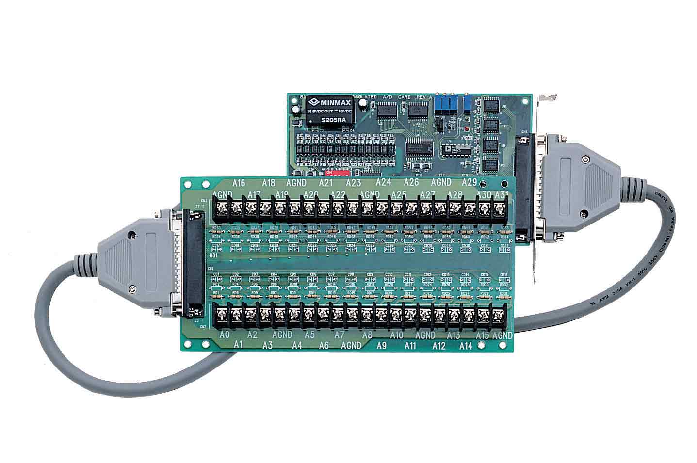
ACLD-9881
LOOKING FOR THE RIGHT
INDUSTRIAL SOLUTION?
Discover embedded, communication and automation solutions tailored to your application.
- 32 isolated single‑ended analog input channels for simultaneous multi‑signal acquisition.
- 12‑bit successive approximation A/D converter (Burr‑Brown AD574 or equivalent).
- High isolation voltage: Over 2500 VDC channel‑to‑system isolation.
- Programmable gain control: Software‑selectable gains of ×1, ×2, ×4, ×8, and ×16.
- Selectable input ranges: Bipolar (±10 V, ±5 V, ±2.5 V, ±1.25 V, ±0.625 V) and unipolar (0–10 V, 0–5 V, 0–2.5 V, 0–1.25 V, 0–0.625 V).
- On‑board signal conditioning circuits for attenuation and current‑to‑voltage conversion.
- Integral DC‑to‑DC converters for isolated power supply stability.
- Compact half‑size ISA card (160 mm × 122 mm).
- High accuracy: 0.015 % of reading ± 1 LSB.
- Conversion speed: Up to 50 kHz.
- Over‑voltage protection: Continuous ±35 V maximum.
- Software trigger mode for flexible data acquisition control.
- 4‑layer PCB with integral ground plane for noise immunity and signal integrity.
- Comprehensive software support: DOS C/C++ library, Windows DLL (ACLS‑DLL2), and LabVIEW driver (ACLS‑LVIEW).
- 12‑bit successive approximation A/D converter (Burr‑Brown AD574 or equivalent).
- High isolation voltage: Over 2500 VDC channel‑to‑system isolation.
- Programmable gain control: Software‑selectable gains of ×1, ×2, ×4, ×8, and ×16.
- Selectable input ranges: Bipolar (±10 V, ±5 V, ±2.5 V, ±1.25 V, ±0.625 V) and unipolar (0–10 V, 0–5 V, 0–2.5 V, 0–1.25 V, 0–0.625 V).
- On‑board signal conditioning circuits for attenuation and current‑to‑voltage conversion.
- Integral DC‑to‑DC converters for isolated power supply stability.
- Compact half‑size ISA card (160 mm × 122 mm).
- High accuracy: 0.015 % of reading ± 1 LSB.
- Conversion speed: Up to 50 kHz.
- Over‑voltage protection: Continuous ±35 V maximum.
- Software trigger mode for flexible data acquisition control.
- 4‑layer PCB with integral ground plane for noise immunity and signal integrity.
- Comprehensive software support: DOS C/C++ library, Windows DLL (ACLS‑DLL2), and LabVIEW driver (ACLS‑LVIEW).
Comprehensive Product Summary: ADLINK ACL‑8113A 12‑bit 32‑Channel Isolated Analog Input ISA Card
### 1. Product Overview
Product Name: ACL‑8113A
Model: ACL‑8113A
Series: NuDAQ ISA‑Bus Data Acquisition Series
Article Number: ACL‑8113A
Manufacturer: ADLINK Technology Inc.
Manufacturer Address: 9F, No. 166, Jian Yi Road, Chungho City, Taipei 235, Taiwan, R.O.C.
Website: [www.adlink.com.tw](http://www.adlink.com.tw)
Support Contacts:
- Sales & Service: service@adlink.com.tw
- Technical Support (NuDAQ): nudaq@adlink.com.tw
- Software Support: sw@adlink.com.tw
- Telephone: +886‑2‑82265877
- Fax: +886‑2‑82265717
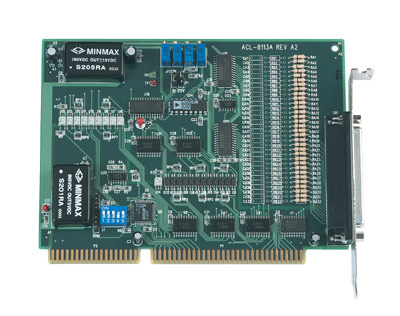
The ADLINK ACL‑8113A is a 12‑bit, 32‑channel single‑ended isolated analog input card designed for the ISA bus. It provides high‑voltage isolation, on‑board signal conditioning, and programmable gain control, making it ideal for industrial measurement, monitoring, and data acquisition applications. The card integrates two DC‑to‑DC converters for stable operation and features a compact half‑size PCB design.
### 2. Key Features
- 32 isolated single‑ended analog input channels for simultaneous multi‑signal acquisition.
- 12‑bit successive approximation A/D converter (Burr‑Brown AD574 or equivalent).
- High isolation voltage: Over 2500 VDC channel‑to‑system isolation.
- Programmable gain control: Software‑selectable gains of ×1, ×2, ×4, ×8, and ×16.
- Selectable input ranges: Bipolar (±10 V, ±5 V, ±2.5 V, ±1.25 V, ±0.625 V) and unipolar (0–10 V, 0–5 V, 0–2.5 V, 0–1.25 V, 0–0.625 V).
- On‑board signal conditioning circuits for attenuation and current‑to‑voltage conversion.
- Integral DC‑to‑DC converters for isolated power supply stability.
- Compact half‑size ISA card (160 mm × 122 mm).
- High accuracy: 0.015 % of reading ± 1 LSB.
- Conversion speed: Up to 50 kHz.
- Over‑voltage protection: Continuous ±35 V maximum.
- Software trigger mode for flexible data acquisition control.
- 4‑layer PCB with integral ground plane for noise immunity and signal integrity.
- Comprehensive software support: DOS C/C++ library, Windows DLL (ACLS‑DLL2), and LabVIEW driver (ACLS‑LVIEW).
### 3. Technical Specifications
Analog Input (A/D):
- Channels: 32 isolated single‑ended inputs
- Resolution: 12 bits
- Input Ranges:
- *10 V Range:*
- Bipolar: ±5 V, ±2.5 V, ±1.25 V, ±0.625 V, ±0.3125 V
- Unipolar: 0–10 V, 0–5 V, 0–2.5 V, 0–1.25 V, 0–0.625 V
- *20 V Range:*
- Bipolar: ±10 V, ±5 V, ±2.5 V, ±1.25 V, ±0.625 V
- Unipolar: 0–10 V, 0–5 V, 0–2.5 V, 0–1.25 V
- Input Impedance: 10 MΩ
- Isolation Voltage: > 2500 VDC
- Over‑voltage Protection: ±35 V continuous
- Converter Type: Successive approximation (AD574 or equivalent)
- Conversion Speed: 50 kHz maximum
- Accuracy: 0.015 % of reading ± 1 LSB
- Non‑linearity: ±1 bit maximum
- Temperature Coefficient: 5 ppm typical, 15 ppm maximum
- Trigger Mode: Software trigger
- Data Transfer: Program control
General Specifications:
- Connector: 37‑pin D‑type female connector
- Operating Temperature: 0 °C – 55 °C
- Storage Temperature: −20 °C – 80 °C
- Humidity: 5 – 95 % RH, non‑condensing
- Power Consumption: +5 V @ 960 mA (max)
- Dimensions: 160 mm (L) × 122 mm (W)
- PCB Type: 4‑layer with ground plane
### 4. Functionality
The ACL‑8113A performs analog‑to‑digital conversion on up to 32 isolated single‑ended channels. Each channel is individually isolated to protect the host PC and connected equipment from high‑voltage transients. The card’s on‑board signal conditioning allows users to attenuate input signals or configure channels for current‑to‑voltage conversion.
Operation Principle:
1. The user selects the input channel via the channel control register.
2. The desired gain and input range are configured through software or jumpers.
3. A software trigger initiates the A/D conversion.
4. The converted 12‑bit digital data is stored in two 8‑bit registers (low and high bytes).
5. The DRDY (Data Ready) bit indicates conversion completion.
Use Cases and Applications:
- Industrial process monitoring and control
- Multi‑channel sensor and transducer data acquisition
- Waveform and transient analysis
- Vibration measurement
- Laboratory instrumentation and test automation
- Signal isolation and protection in mixed‑voltage environments
Compatibility:
- ISA bus interface (16 consecutive I/O addresses required)
- Compatible with DOS, Windows 95/98/NT environments
- Supported by ADLINK’s NuDAQ software suite, C/C++ libraries, and LabVIEW drivers
### 5. Components & Accessories
Package Contents:
- ACL‑8113A 32‑Channel Isolated A/D Card
- ADLINK Software CD (includes DOS library, ACLS‑DLL2, ACLS‑LVIEW drivers, and documentation)
- User’s Manual
Connector:
- DB‑37 Female Connector Pinout:
- Channels AI0–AI31 (Analog Inputs)
- Analog Ground (A.GND) pins interleaved for reference stability
Optional Accessories:
- Shielded analog input cables (DB‑37 to terminal block)
- External signal conditioning modules
- Calibration tools (multimeter, voltage calibrator)
### 6. Installation & Setup
System Requirements:
- IBM‑PC compatible system with available ISA slot
- +5 V power supply (960 mA max)
- Supported OS: DOS, Windows 95/98/NT
Installation Steps:
1. Unpacking: Handle the card on a grounded anti‑static mat using an ESD wrist strap.
2. Base Address Configuration:
- Selectable via 5‑position DIP switch (SW1).
- Default base address: Hex 220.
- Address range: 000h – 3F0h (16 consecutive I/O addresses).
3. Input Range Selection:
- JP1: Selects voltage range (±10 V or ±20 V).
- JP2: Selects input polarity (Bipolar or Unipolar).
4. Gain Control: Software‑programmable via register (BASE + 9).
5. Connector Wiring: Connect analog inputs to DB‑37 pins according to pin assignment.
6. Software Installation:
- Insert ADLINK CD.
- Run `SETUP` from `\NuDAQISA\8113` directory.
- Install DOS library or Windows drivers as required.
Calibration:
- Four variable resistors (VR1–VR4) for fine adjustment:
- VR1: A/D bipolar offset
- VR2: A/D bipolar full‑scale
- VR3: Amplifier offset
- VR4: A/D unipolar full‑scale
- Calibration requires a 6½‑digit multimeter and stable DC voltage source.
### 7. Performance & Capabilities
A/D Conversion Performance:
- Resolution: 12 bits (4096 discrete levels)
- Sampling Rate: Up to 50 kHz (software‑triggered)
- Accuracy: 0.015 % ± 1 LSB
- Gain Settings: ×1, ×2, ×4, ×8, ×16
- Input Impedance: 10 MΩ
- Isolation: 2500 VDC minimum
- Over‑voltage Protection: ±35 V continuous
Data Handling:
- Registers:
- BASE + 4: A/D low byte
- BASE + 5: A/D high byte (includes DRDY bit)
- BASE + 9: Gain control
- BASE + 10: Channel control
- BASE + 12: Software trigger
- Data Format: 12‑bit binary (0–4095).
- Voltage Conversion Formula:
- Bipolar ±10 V: V = (AD_Data × 20 / (4096 × Gain)) – (10 / Gain)
- Bipolar ±5 V: V = (AD_Data × 10 / (4096 × Gain)) – (5 / Gain)
- Unipolar 0–10 V: V = (AD_Data × 10 / (4096 × Gain))
Limitations:
- Software‑triggered only (no hardware trigger).
- Single‑ended input configuration (no differential mode).
- Conversion rate limited by software polling.
### 8. Standards & Compliance
- Bus Interface: ISA (Industry Standard Architecture)
- Isolation: > 2500 VDC channel‑to‑system
- Over‑voltage Protection: ±35 V continuous
- Environmental Compliance:
- Operating: 0 °C – 55 °C
- Storage: −20 °C – 80 °C
- Humidity: 5 – 95 % non‑condensing
- PCB Design: 4‑layer with ground plane for EMI reduction
- Software Compatibility:
- DOS C/C++ library
- Windows 95/98/NT DLL (ACLS‑DLL2)
- LabVIEW driver (ACLS‑LVIEW)
- Industry Standards:
- ISA bus electrical and mechanical specifications
- CE‑compliant design practices (for noise immunity and safety)
### 9. Additional Information
Software Support:
- DOS Library: Includes initialization, channel selection, gain control, and A/D acquisition functions.
- Windows DLL (ACLS‑DLL2): Supports VC++, VB, Delphi environments.
- LabVIEW Driver (ACLS‑LVIEW): Provides VIs for integration with NI LabVIEW.
- Example Functions:
- `_8113_Initial()` – Initialize card
- `_8113_ActCard_Set()` – Select active card
- `_8113_Channel_Select()` / `_8113_Channel_Clear()` – Manage channels
- `_8113_Gain_Select()` – Set gain
- `_8113_AD_Acquire()` – Acquire single channel data
- `_8113_MAD_Acquire()` – Acquire multiple channel data
Maintenance & Calibration:
- Periodic calibration recommended for accuracy.
- Use VR1–VR4 adjustments as per calibration procedure.
- Ensure anti‑static handling during maintenance.
Warranty:
- Duration: 1 year from date of purchase.
- Coverage: Defects in materials and workmanship.
- Exclusions:
- Damage due to misuse, modification, or operation beyond specifications.
- Units with removed or altered serial numbers.
- Service Procedure:
- Return product postage‑prepaid with proof of purchase.
- Manufacturer may repair or replace at its discretion.
- Liability limited to original purchase price.
Support & Service:
- Technical assistance available via email and phone.
- Users encouraged to provide detailed system information (OS, CPU, chipset, BIOS, etc.) when requesting support.
### Summary
The ADLINK ACL‑8113A is a robust, high‑isolation, 12‑bit, 32‑channel analog input card for ISA‑bus systems. It combines precision A/D conversion, flexible input range selection, and software‑programmable gain control in a compact, industrial‑grade design. With its 2500 VDC isolation, ±35 V over‑voltage protection, and comprehensive software support, the ACL‑8113A is ideally suited for industrial measurement, process monitoring, and laboratory data acquisition applications requiring reliable, high‑accuracy analog input performance.

### 1. Product Overview
Product Name: ACL‑8113A
Model: ACL‑8113A
Series: NuDAQ ISA‑Bus Data Acquisition Series
Article Number: ACL‑8113A
Manufacturer: ADLINK Technology Inc.
Manufacturer Address: 9F, No. 166, Jian Yi Road, Chungho City, Taipei 235, Taiwan, R.O.C.
Website: [www.adlink.com.tw](http://www.adlink.com.tw)
Support Contacts:
- Sales & Service: service@adlink.com.tw
- Technical Support (NuDAQ): nudaq@adlink.com.tw
- Software Support: sw@adlink.com.tw
- Telephone: +886‑2‑82265877
- Fax: +886‑2‑82265717
The ADLINK ACL‑8113A is a 12‑bit, 32‑channel single‑ended isolated analog input card designed for the ISA bus. It provides high‑voltage isolation, on‑board signal conditioning, and programmable gain control, making it ideal for industrial measurement, monitoring, and data acquisition applications. The card integrates two DC‑to‑DC converters for stable operation and features a compact half‑size PCB design.
### 2. Key Features
- 32 isolated single‑ended analog input channels for simultaneous multi‑signal acquisition.
- 12‑bit successive approximation A/D converter (Burr‑Brown AD574 or equivalent).
- High isolation voltage: Over 2500 VDC channel‑to‑system isolation.
- Programmable gain control: Software‑selectable gains of ×1, ×2, ×4, ×8, and ×16.
- Selectable input ranges: Bipolar (±10 V, ±5 V, ±2.5 V, ±1.25 V, ±0.625 V) and unipolar (0–10 V, 0–5 V, 0–2.5 V, 0–1.25 V, 0–0.625 V).
- On‑board signal conditioning circuits for attenuation and current‑to‑voltage conversion.
- Integral DC‑to‑DC converters for isolated power supply stability.
- Compact half‑size ISA card (160 mm × 122 mm).
- High accuracy: 0.015 % of reading ± 1 LSB.
- Conversion speed: Up to 50 kHz.
- Over‑voltage protection: Continuous ±35 V maximum.
- Software trigger mode for flexible data acquisition control.
- 4‑layer PCB with integral ground plane for noise immunity and signal integrity.
- Comprehensive software support: DOS C/C++ library, Windows DLL (ACLS‑DLL2), and LabVIEW driver (ACLS‑LVIEW).
### 3. Technical Specifications
Analog Input (A/D):
- Channels: 32 isolated single‑ended inputs
- Resolution: 12 bits
- Input Ranges:
- *10 V Range:*
- Bipolar: ±5 V, ±2.5 V, ±1.25 V, ±0.625 V, ±0.3125 V
- Unipolar: 0–10 V, 0–5 V, 0–2.5 V, 0–1.25 V, 0–0.625 V
- *20 V Range:*
- Bipolar: ±10 V, ±5 V, ±2.5 V, ±1.25 V, ±0.625 V
- Unipolar: 0–10 V, 0–5 V, 0–2.5 V, 0–1.25 V
- Input Impedance: 10 MΩ
- Isolation Voltage: > 2500 VDC
- Over‑voltage Protection: ±35 V continuous
- Converter Type: Successive approximation (AD574 or equivalent)
- Conversion Speed: 50 kHz maximum
- Accuracy: 0.015 % of reading ± 1 LSB
- Non‑linearity: ±1 bit maximum
- Temperature Coefficient: 5 ppm typical, 15 ppm maximum
- Trigger Mode: Software trigger
- Data Transfer: Program control
General Specifications:
- Connector: 37‑pin D‑type female connector
- Operating Temperature: 0 °C – 55 °C
- Storage Temperature: −20 °C – 80 °C
- Humidity: 5 – 95 % RH, non‑condensing
- Power Consumption: +5 V @ 960 mA (max)
- Dimensions: 160 mm (L) × 122 mm (W)
- PCB Type: 4‑layer with ground plane
### 4. Functionality
The ACL‑8113A performs analog‑to‑digital conversion on up to 32 isolated single‑ended channels. Each channel is individually isolated to protect the host PC and connected equipment from high‑voltage transients. The card’s on‑board signal conditioning allows users to attenuate input signals or configure channels for current‑to‑voltage conversion.
Operation Principle:
1. The user selects the input channel via the channel control register.
2. The desired gain and input range are configured through software or jumpers.
3. A software trigger initiates the A/D conversion.
4. The converted 12‑bit digital data is stored in two 8‑bit registers (low and high bytes).
5. The DRDY (Data Ready) bit indicates conversion completion.
Use Cases and Applications:
- Industrial process monitoring and control
- Multi‑channel sensor and transducer data acquisition
- Waveform and transient analysis
- Vibration measurement
- Laboratory instrumentation and test automation
- Signal isolation and protection in mixed‑voltage environments
Compatibility:
- ISA bus interface (16 consecutive I/O addresses required)
- Compatible with DOS, Windows 95/98/NT environments
- Supported by ADLINK’s NuDAQ software suite, C/C++ libraries, and LabVIEW drivers
### 5. Components & Accessories
Package Contents:
- ACL‑8113A 32‑Channel Isolated A/D Card
- ADLINK Software CD (includes DOS library, ACLS‑DLL2, ACLS‑LVIEW drivers, and documentation)
- User’s Manual
Connector:
- DB‑37 Female Connector Pinout:
- Channels AI0–AI31 (Analog Inputs)
- Analog Ground (A.GND) pins interleaved for reference stability
Optional Accessories:
- Shielded analog input cables (DB‑37 to terminal block)
- External signal conditioning modules
- Calibration tools (multimeter, voltage calibrator)
### 6. Installation & Setup
System Requirements:
- IBM‑PC compatible system with available ISA slot
- +5 V power supply (960 mA max)
- Supported OS: DOS, Windows 95/98/NT
Installation Steps:
1. Unpacking: Handle the card on a grounded anti‑static mat using an ESD wrist strap.
2. Base Address Configuration:
- Selectable via 5‑position DIP switch (SW1).
- Default base address: Hex 220.
- Address range: 000h – 3F0h (16 consecutive I/O addresses).
3. Input Range Selection:
- JP1: Selects voltage range (±10 V or ±20 V).
- JP2: Selects input polarity (Bipolar or Unipolar).
4. Gain Control: Software‑programmable via register (BASE + 9).
5. Connector Wiring: Connect analog inputs to DB‑37 pins according to pin assignment.
6. Software Installation:
- Insert ADLINK CD.
- Run `SETUP` from `\NuDAQISA\8113` directory.
- Install DOS library or Windows drivers as required.
Calibration:
- Four variable resistors (VR1–VR4) for fine adjustment:
- VR1: A/D bipolar offset
- VR2: A/D bipolar full‑scale
- VR3: Amplifier offset
- VR4: A/D unipolar full‑scale
- Calibration requires a 6½‑digit multimeter and stable DC voltage source.
### 7. Performance & Capabilities
A/D Conversion Performance:
- Resolution: 12 bits (4096 discrete levels)
- Sampling Rate: Up to 50 kHz (software‑triggered)
- Accuracy: 0.015 % ± 1 LSB
- Gain Settings: ×1, ×2, ×4, ×8, ×16
- Input Impedance: 10 MΩ
- Isolation: 2500 VDC minimum
- Over‑voltage Protection: ±35 V continuous
Data Handling:
- Registers:
- BASE + 4: A/D low byte
- BASE + 5: A/D high byte (includes DRDY bit)
- BASE + 9: Gain control
- BASE + 10: Channel control
- BASE + 12: Software trigger
- Data Format: 12‑bit binary (0–4095).
- Voltage Conversion Formula:
- Bipolar ±10 V: V = (AD_Data × 20 / (4096 × Gain)) – (10 / Gain)
- Bipolar ±5 V: V = (AD_Data × 10 / (4096 × Gain)) – (5 / Gain)
- Unipolar 0–10 V: V = (AD_Data × 10 / (4096 × Gain))
Limitations:
- Software‑triggered only (no hardware trigger).
- Single‑ended input configuration (no differential mode).
- Conversion rate limited by software polling.
### 8. Standards & Compliance
- Bus Interface: ISA (Industry Standard Architecture)
- Isolation: > 2500 VDC channel‑to‑system
- Over‑voltage Protection: ±35 V continuous
- Environmental Compliance:
- Operating: 0 °C – 55 °C
- Storage: −20 °C – 80 °C
- Humidity: 5 – 95 % non‑condensing
- PCB Design: 4‑layer with ground plane for EMI reduction
- Software Compatibility:
- DOS C/C++ library
- Windows 95/98/NT DLL (ACLS‑DLL2)
- LabVIEW driver (ACLS‑LVIEW)
- Industry Standards:
- ISA bus electrical and mechanical specifications
- CE‑compliant design practices (for noise immunity and safety)
### 9. Additional Information
Software Support:
- DOS Library: Includes initialization, channel selection, gain control, and A/D acquisition functions.
- Windows DLL (ACLS‑DLL2): Supports VC++, VB, Delphi environments.
- LabVIEW Driver (ACLS‑LVIEW): Provides VIs for integration with NI LabVIEW.
- Example Functions:
- `_8113_Initial()` – Initialize card
- `_8113_ActCard_Set()` – Select active card
- `_8113_Channel_Select()` / `_8113_Channel_Clear()` – Manage channels
- `_8113_Gain_Select()` – Set gain
- `_8113_AD_Acquire()` – Acquire single channel data
- `_8113_MAD_Acquire()` – Acquire multiple channel data
Maintenance & Calibration:
- Periodic calibration recommended for accuracy.
- Use VR1–VR4 adjustments as per calibration procedure.
- Ensure anti‑static handling during maintenance.
Warranty:
- Duration: 1 year from date of purchase.
- Coverage: Defects in materials and workmanship.
- Exclusions:
- Damage due to misuse, modification, or operation beyond specifications.
- Units with removed or altered serial numbers.
- Service Procedure:
- Return product postage‑prepaid with proof of purchase.
- Manufacturer may repair or replace at its discretion.
- Liability limited to original purchase price.
Support & Service:
- Technical assistance available via email and phone.
- Users encouraged to provide detailed system information (OS, CPU, chipset, BIOS, etc.) when requesting support.
### Summary
The ADLINK ACL‑8113A is a robust, high‑isolation, 12‑bit, 32‑channel analog input card for ISA‑bus systems. It combines precision A/D conversion, flexible input range selection, and software‑programmable gain control in a compact, industrial‑grade design. With its 2500 VDC isolation, ±35 V over‑voltage protection, and comprehensive software support, the ACL‑8113A is ideally suited for industrial measurement, process monitoring, and laboratory data acquisition applications requiring reliable, high‑accuracy analog input performance.
-
A8113 Manual.PDF
Manual
- ACLD-9881 - Panel for mounting low pass filter etc., incl. ACL-10137-1
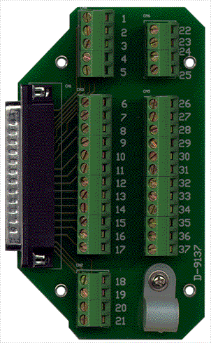
- ACLD-9137-01 - Direct 37 small screw terminal
- DIN-37D-01 - 37pin D-type panel DIN rail w/o cable