WD-DASK
LOOKING FOR THE RIGHT
INDUSTRIAL SOLUTION?
Discover embedded, communication and automation solutions tailored to your application.
- High-Speed Sampling: Up to 80 MS/s per channel with simultaneous acquisition across all four channels.
- High Resolution: 12-bit analog-to-digital conversion for accurate signal representation.
- Wide Bandwidth: 40 MHz analog input bandwidth supporting high-frequency signal capture.
- Large Onboard Memory: 1 GB shared memory for extended recording durations at maximum sampling rates.
- Programmable Input Ranges: ±0.5 V, ±1 V, ±5 V, and ±10 V ranges selectable via software.
- Selectable Input Impedance: 50 Ω or 1 MΩ, software-configurable for flexible signal interfacing.
- Digital Filtering: FPGA-based 10 MHz or 20 MHz digital filters for noise reduction and signal conditioning.
- Scatter-Gather DMA: High-speed, low-overhead data transfer directly to host memory without CPU intervention.
- Triggering Flexibility: Supports software, analog, external digital, and SSI (System Synchronization Interface) triggers.
- Synchronization Support: Three synchronous digital inputs (SDI) and SSI bus for multi-card synchronization.
- Auto-Calibration: Fully automated calibration with onboard precision voltage references.
- Software Support: Compatible with Windows 7/8 (x86/x64) and Linux; SDKs for LabVIEW, MATLAB, C/C++, Visual Basic, and Visual Studio.NET.
- Environmental Compliance: RoHS and WEEE compliant; CE and FCC Class A certified.
- Variant Option: PCIe-9814P includes a PLL module for precise synchronization using an external 10 MHz reference clock.
- High Resolution: 12-bit analog-to-digital conversion for accurate signal representation.
- Wide Bandwidth: 40 MHz analog input bandwidth supporting high-frequency signal capture.
- Large Onboard Memory: 1 GB shared memory for extended recording durations at maximum sampling rates.
- Programmable Input Ranges: ±0.5 V, ±1 V, ±5 V, and ±10 V ranges selectable via software.
- Selectable Input Impedance: 50 Ω or 1 MΩ, software-configurable for flexible signal interfacing.
- Digital Filtering: FPGA-based 10 MHz or 20 MHz digital filters for noise reduction and signal conditioning.
- Scatter-Gather DMA: High-speed, low-overhead data transfer directly to host memory without CPU intervention.
- Triggering Flexibility: Supports software, analog, external digital, and SSI (System Synchronization Interface) triggers.
- Synchronization Support: Three synchronous digital inputs (SDI) and SSI bus for multi-card synchronization.
- Auto-Calibration: Fully automated calibration with onboard precision voltage references.
- Software Support: Compatible with Windows 7/8 (x86/x64) and Linux; SDKs for LabVIEW, MATLAB, C/C++, Visual Basic, and Visual Studio.NET.
- Environmental Compliance: RoHS and WEEE compliant; CE and FCC Class A certified.
- Variant Option: PCIe-9814P includes a PLL module for precise synchronization using an external 10 MHz reference clock.
Comprehensive Product Summary: ADLINK PCIe-9814 4-CH 12-Bit 80 MS/s PCI Express Digitizer
### 1. Product Overview
Product Name: PCIe-9814
Model: PCIe-9814 / PCIe-9814P (variant with PLL module)
Series: PCI Express Digitizer Series
Article Number: PCIe-9814
Manufacturer: ADLINK Technology, Inc.
Part Number: 50-11256-1000
Manual Revision: 2.00 (February 13, 2015)
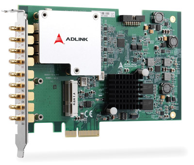
The ADLINK PCIe-9814 is a high-performance PCI Express (PCIe) x4 lane analog-to-digital (AD) acquisition card designed for high-speed, high-resolution data digitization. It features four simultaneous analog input channels, each capable of 80 mega-samples per second (MS/s) with 12-bit resolution. The card integrates 1 GB of onboard memory, advanced triggering modes, and scatter-gather DMA for efficient data streaming. It is ideal for applications requiring precise, synchronized, and continuous data capture such as radar, LiDAR, power monitoring, and non-destructive testing.
### 2. Key Features
- High-Speed Sampling: Up to 80 MS/s per channel with simultaneous acquisition across all four channels.
- High Resolution: 12-bit analog-to-digital conversion for accurate signal representation.
- Wide Bandwidth: 40 MHz analog input bandwidth supporting high-frequency signal capture.
- Large Onboard Memory: 1 GB shared memory for extended recording durations at maximum sampling rates.
- Programmable Input Ranges: ±0.5 V, ±1 V, ±5 V, and ±10 V ranges selectable via software.
- Selectable Input Impedance: 50 Ω or 1 MΩ, software-configurable for flexible signal interfacing.
- Digital Filtering: FPGA-based 10 MHz or 20 MHz digital filters for noise reduction and signal conditioning.
- Scatter-Gather DMA: High-speed, low-overhead data transfer directly to host memory without CPU intervention.
- Triggering Flexibility: Supports software, analog, external digital, and SSI (System Synchronization Interface) triggers.
- Synchronization Support: Three synchronous digital inputs (SDI) and SSI bus for multi-card synchronization.
- Auto-Calibration: Fully automated calibration with onboard precision voltage references.
- Software Support: Compatible with Windows 7/8 (x86/x64) and Linux; SDKs for LabVIEW, MATLAB, C/C++, Visual Basic, and Visual Studio.NET.
- Environmental Compliance: RoHS and WEEE compliant; CE and FCC Class A certified.
- Variant Option: PCIe-9814P includes a PLL module for precise synchronization using an external 10 MHz reference clock.
### 3. Technical Specifications
Analog Input:
- Channels: 4 single-ended
- Connector Type: SMB (Snap-on)
- Input Coupling: DC
- Input Impedance: 50 Ω or 1 MΩ (software selectable)
- Input Voltage Ranges: ±0.5 V, ±1 V, ±5 V, ±10 V
- Bandwidth (-3 dB): 40 MHz
- ADC Resolution: 12 bits
- Overvoltage Protection: ±30 V @ 1 MΩ (±5 V/±10 V ranges), ±10 V sine wave @ 50 Ω
- Crosstalk: -80 dB (±0.5 V), -90 dB (±1 V, ±5 V, ±10 V)
- System Noise (RMS): 150 µV (±0.5 V), 300 µV (±1 V), 1.5 mV (±5 V), 2.5 mV (±10 V)
- Offset Error: ±0.5 mV (±0.5 V/±1 V), ±4 mV (±5 V), ±10 mV (±10 V)
- Gain Error: ±1% (50 Ω all ranges), ±0.5% (1 MΩ ±0.5 V/±1 V/±5 V), ±1% (1 MΩ ±10 V)
Spectral Performance (10 MHz, -1 dBFS input):
- SNR: 64–65 dB
- THD: -74 dB (filter off), -93 dB (filter on)
- SFDR: 72–78 dB depending on impedance and filter settings
Trigger System:
- Sources: Software, external digital, analog (CH0–CH3), SSI
- Modes: Post-trigger, pre-trigger, middle trigger, delay trigger, re-trigger
- External Trigger Input: SMB connector, 3.3 V TTL (5 V tolerant), 20 ns minimum pulse width
- Thresholds: VIH = 2.0 V, VIL = 0.8 V
- Polarity: Rising or falling edge selectable
Timebase:
- Internal Clock: 1.22 kHz to 80 MHz (±25 ppm accuracy)
- External Clock Input: 20 MHz to 80 MHz, 1–5 Vpp
- External Reference Clock (PCIe-9814P only): 10 MHz, 3.3–5 V TTL
- Warm-up Time: 15 minutes recommended
Data Storage & Transfer:
- Onboard Memory: 1 GB shared among channels
- DMA: Scatter-Gather supported for continuous streaming
- Reference Voltages: +1.8 V, +0.9 V, +0.45 V (<3 ppm/°C drift)
Physical & Environmental:
- Dimensions: 167.64 mm (W) × 106.68 mm (H) [6.53” × 4.16”]
- Weight: Approx. 200 g (typical)
- Operating Temperature: 0°C to 50°C
- Storage Temperature: -20°C to 80°C
- Humidity: 10–90% RH, non-condensing
- Power Consumption:
- PCIe-9814: 5.12 W (standby), 6.13 W (full load)
- PCIe-9814P: 7.93 W (standby), 8.65 W (full load)
- Power Rails: +3.3 V @ 20 mA, +12 V @ 425–715 mA
Bus Interface:
- PCI Express Gen 1 x4 (compatible with x4/x8/x16 slots)
### 4. Functionality
The PCIe-9814 digitizer converts analog signals into high-resolution digital data streams for analysis and processing. Each channel operates independently yet synchronously, ensuring zero inter-channel phase delay. The onboard FPGA manages digital filtering, triggering logic, and DMA control. Data is buffered in onboard memory before being transferred to the host system via PCIe bus-mastering DMA.
Use Cases:
- Power system monitoring and partial discharge analysis
- Radar and LiDAR signal acquisition
- Non-destructive testing (NDT)
- High-speed transient signal capture
- Mixed-signal acquisition with synchronous digital inputs
Compatibility:
- Operating Systems: Windows 7/8 (x86/x64), Linux
- Software Environments: WD-DASK, LabVIEW, MATLAB, C/C++, Visual Basic, Visual Studio.NET
### 5. Components & Accessories
Included Items:
- PCIe-9814 or PCIe-9814P digitizer card
- ADLINK All-in-One software CD
- Quick Start Guide
Optional Accessories:
- ACL-eSSI-2/3/4 cables for multi-card synchronization (2, 3, or 4 devices)
- SMB coaxial cables for analog and trigger connections
Connectors (Front Panel):
- 4 × SMB for analog inputs (CH0–CH3)
- 1 × SMB for external trigger input
- 1 × SMB for external sample clock input (CLK IN)
- 3 × SMB for synchronous digital inputs (SDI0–SDI2)
### 6. Installation & Setup
Requirements:
- Available PCI Express x4, x8, or x16 slot
- Anti-static handling environment
- Phillips screwdriver and anti-static wrist strap
Installation Steps:
1. Power off the host PC and remove the cover.
2. Insert the PCIe-9814 into an available PCIe slot.
3. Secure the bracket with the retaining screw.
4. Replace the cover and power on the system.
5. Install drivers and software from the ADLINK All-in-One CD.
Configuration:
- Input impedance, voltage range, and trigger modes are software-configurable.
- Card numbering for multi-module setups is set via DIP switches (0–15).
- Auto-calibration is performed automatically at startup or via software command.
### 7. Performance & Capabilities
- Sampling Rate: 1.22 kS/s to 80 MS/s per channel
- Resolution: 12 bits
- Bandwidth: 40 MHz (-3 dB)
- Dynamic Range: Up to 78 dB SFDR
- Data Throughput: Up to 250 MB/s per PCIe lane (x4 lanes total)
- DMA Transfer: Continuous streaming with scatter-gather mode; supports multi-buffered DMA
- Trigger Latency: <20 ns (digital trigger)
- Synchronization: Multi-card synchronization via SSI and SDI interfaces
- Limitations: External clock frequency limited to 20–80 MHz; external trigger pulse width ≥20 ns
### 8. Standards & Compliance
- Electrical & EMC: CE, FCC Class A
- Environmental: RoHS and WEEE compliant
- Bus Interface: PCI Express Gen 1 x4 standard
- Safety: Designed for industrial and laboratory environments (0–50°C operation)
- Calibration: Factory-calibrated with EEPROM-stored constants; auto-calibration supported
### 9. Additional Information
Warranty & Support:
- Standard ADLINK warranty (contact regional office for details)
- Global technical support via email and phone
- Firmware updates supported via software (multi-boot recovery switch available)
Maintenance:
- Periodic auto-calibration recommended after installation or temperature changes
- Warm-up time: 15–20 minutes before precision measurements
- Clean connectors with dry air; avoid moisture and static discharge
Software & Updates:
- WD-DASK driver package for Windows (DLL-based API)
- DAQPilot and DAQLite toolkits for LabVIEW integration
- Linux driver support available
- Firmware updates via ADLINK utilities; recovery via SW2 switch if update fails
Environmental Responsibility:
- ADLINK adheres to RoHS and WEEE directives
- Products designed for minimal environmental impact and recyclability
Manufacturer Contact:
ADLINK Technology, Inc.
9F, No.166 Jian Yi Road, Zhonghe District, New Taipei City 235, Taiwan
Tel: +886-2-8226-5877 | Email: service@adlinktech.com
Regional offices available in the USA, China, Japan, Germany, France, Korea, Singapore, India, Israel, and the UK.
### Summary
The ADLINK PCIe-9814 is a robust, high-speed, 4-channel PCI Express digitizer engineered for precision data acquisition in demanding applications. With 12-bit resolution, 80 MS/s sampling, and 1 GB onboard memory, it delivers exceptional performance for real-time signal capture and analysis. Its flexible triggering, synchronization, and software integration capabilities make it suitable for advanced test, measurement, and research environments. The PCIe-9814P variant further enhances synchronization accuracy with a PLL-based external reference clock, ensuring precise timing across multiple modules.
This digitizer exemplifies ADLINK’s commitment to high-quality, reliable, and environmentally responsible instrumentation solutions for industrial and scientific applications.

### 1. Product Overview
Product Name: PCIe-9814
Model: PCIe-9814 / PCIe-9814P (variant with PLL module)
Series: PCI Express Digitizer Series
Article Number: PCIe-9814
Manufacturer: ADLINK Technology, Inc.
Part Number: 50-11256-1000
Manual Revision: 2.00 (February 13, 2015)
The ADLINK PCIe-9814 is a high-performance PCI Express (PCIe) x4 lane analog-to-digital (AD) acquisition card designed for high-speed, high-resolution data digitization. It features four simultaneous analog input channels, each capable of 80 mega-samples per second (MS/s) with 12-bit resolution. The card integrates 1 GB of onboard memory, advanced triggering modes, and scatter-gather DMA for efficient data streaming. It is ideal for applications requiring precise, synchronized, and continuous data capture such as radar, LiDAR, power monitoring, and non-destructive testing.
### 2. Key Features
- High-Speed Sampling: Up to 80 MS/s per channel with simultaneous acquisition across all four channels.
- High Resolution: 12-bit analog-to-digital conversion for accurate signal representation.
- Wide Bandwidth: 40 MHz analog input bandwidth supporting high-frequency signal capture.
- Large Onboard Memory: 1 GB shared memory for extended recording durations at maximum sampling rates.
- Programmable Input Ranges: ±0.5 V, ±1 V, ±5 V, and ±10 V ranges selectable via software.
- Selectable Input Impedance: 50 Ω or 1 MΩ, software-configurable for flexible signal interfacing.
- Digital Filtering: FPGA-based 10 MHz or 20 MHz digital filters for noise reduction and signal conditioning.
- Scatter-Gather DMA: High-speed, low-overhead data transfer directly to host memory without CPU intervention.
- Triggering Flexibility: Supports software, analog, external digital, and SSI (System Synchronization Interface) triggers.
- Synchronization Support: Three synchronous digital inputs (SDI) and SSI bus for multi-card synchronization.
- Auto-Calibration: Fully automated calibration with onboard precision voltage references.
- Software Support: Compatible with Windows 7/8 (x86/x64) and Linux; SDKs for LabVIEW, MATLAB, C/C++, Visual Basic, and Visual Studio.NET.
- Environmental Compliance: RoHS and WEEE compliant; CE and FCC Class A certified.
- Variant Option: PCIe-9814P includes a PLL module for precise synchronization using an external 10 MHz reference clock.
### 3. Technical Specifications
Analog Input:
- Channels: 4 single-ended
- Connector Type: SMB (Snap-on)
- Input Coupling: DC
- Input Impedance: 50 Ω or 1 MΩ (software selectable)
- Input Voltage Ranges: ±0.5 V, ±1 V, ±5 V, ±10 V
- Bandwidth (-3 dB): 40 MHz
- ADC Resolution: 12 bits
- Overvoltage Protection: ±30 V @ 1 MΩ (±5 V/±10 V ranges), ±10 V sine wave @ 50 Ω
- Crosstalk: -80 dB (±0.5 V), -90 dB (±1 V, ±5 V, ±10 V)
- System Noise (RMS): 150 µV (±0.5 V), 300 µV (±1 V), 1.5 mV (±5 V), 2.5 mV (±10 V)
- Offset Error: ±0.5 mV (±0.5 V/±1 V), ±4 mV (±5 V), ±10 mV (±10 V)
- Gain Error: ±1% (50 Ω all ranges), ±0.5% (1 MΩ ±0.5 V/±1 V/±5 V), ±1% (1 MΩ ±10 V)
Spectral Performance (10 MHz, -1 dBFS input):
- SNR: 64–65 dB
- THD: -74 dB (filter off), -93 dB (filter on)
- SFDR: 72–78 dB depending on impedance and filter settings
Trigger System:
- Sources: Software, external digital, analog (CH0–CH3), SSI
- Modes: Post-trigger, pre-trigger, middle trigger, delay trigger, re-trigger
- External Trigger Input: SMB connector, 3.3 V TTL (5 V tolerant), 20 ns minimum pulse width
- Thresholds: VIH = 2.0 V, VIL = 0.8 V
- Polarity: Rising or falling edge selectable
Timebase:
- Internal Clock: 1.22 kHz to 80 MHz (±25 ppm accuracy)
- External Clock Input: 20 MHz to 80 MHz, 1–5 Vpp
- External Reference Clock (PCIe-9814P only): 10 MHz, 3.3–5 V TTL
- Warm-up Time: 15 minutes recommended
Data Storage & Transfer:
- Onboard Memory: 1 GB shared among channels
- DMA: Scatter-Gather supported for continuous streaming
- Reference Voltages: +1.8 V, +0.9 V, +0.45 V (<3 ppm/°C drift)
Physical & Environmental:
- Dimensions: 167.64 mm (W) × 106.68 mm (H) [6.53” × 4.16”]
- Weight: Approx. 200 g (typical)
- Operating Temperature: 0°C to 50°C
- Storage Temperature: -20°C to 80°C
- Humidity: 10–90% RH, non-condensing
- Power Consumption:
- PCIe-9814: 5.12 W (standby), 6.13 W (full load)
- PCIe-9814P: 7.93 W (standby), 8.65 W (full load)
- Power Rails: +3.3 V @ 20 mA, +12 V @ 425–715 mA
Bus Interface:
- PCI Express Gen 1 x4 (compatible with x4/x8/x16 slots)
### 4. Functionality
The PCIe-9814 digitizer converts analog signals into high-resolution digital data streams for analysis and processing. Each channel operates independently yet synchronously, ensuring zero inter-channel phase delay. The onboard FPGA manages digital filtering, triggering logic, and DMA control. Data is buffered in onboard memory before being transferred to the host system via PCIe bus-mastering DMA.
Use Cases:
- Power system monitoring and partial discharge analysis
- Radar and LiDAR signal acquisition
- Non-destructive testing (NDT)
- High-speed transient signal capture
- Mixed-signal acquisition with synchronous digital inputs
Compatibility:
- Operating Systems: Windows 7/8 (x86/x64), Linux
- Software Environments: WD-DASK, LabVIEW, MATLAB, C/C++, Visual Basic, Visual Studio.NET
### 5. Components & Accessories
Included Items:
- PCIe-9814 or PCIe-9814P digitizer card
- ADLINK All-in-One software CD
- Quick Start Guide
Optional Accessories:
- ACL-eSSI-2/3/4 cables for multi-card synchronization (2, 3, or 4 devices)
- SMB coaxial cables for analog and trigger connections
Connectors (Front Panel):
- 4 × SMB for analog inputs (CH0–CH3)
- 1 × SMB for external trigger input
- 1 × SMB for external sample clock input (CLK IN)
- 3 × SMB for synchronous digital inputs (SDI0–SDI2)
### 6. Installation & Setup
Requirements:
- Available PCI Express x4, x8, or x16 slot
- Anti-static handling environment
- Phillips screwdriver and anti-static wrist strap
Installation Steps:
1. Power off the host PC and remove the cover.
2. Insert the PCIe-9814 into an available PCIe slot.
3. Secure the bracket with the retaining screw.
4. Replace the cover and power on the system.
5. Install drivers and software from the ADLINK All-in-One CD.
Configuration:
- Input impedance, voltage range, and trigger modes are software-configurable.
- Card numbering for multi-module setups is set via DIP switches (0–15).
- Auto-calibration is performed automatically at startup or via software command.
### 7. Performance & Capabilities
- Sampling Rate: 1.22 kS/s to 80 MS/s per channel
- Resolution: 12 bits
- Bandwidth: 40 MHz (-3 dB)
- Dynamic Range: Up to 78 dB SFDR
- Data Throughput: Up to 250 MB/s per PCIe lane (x4 lanes total)
- DMA Transfer: Continuous streaming with scatter-gather mode; supports multi-buffered DMA
- Trigger Latency: <20 ns (digital trigger)
- Synchronization: Multi-card synchronization via SSI and SDI interfaces
- Limitations: External clock frequency limited to 20–80 MHz; external trigger pulse width ≥20 ns
### 8. Standards & Compliance
- Electrical & EMC: CE, FCC Class A
- Environmental: RoHS and WEEE compliant
- Bus Interface: PCI Express Gen 1 x4 standard
- Safety: Designed for industrial and laboratory environments (0–50°C operation)
- Calibration: Factory-calibrated with EEPROM-stored constants; auto-calibration supported
### 9. Additional Information
Warranty & Support:
- Standard ADLINK warranty (contact regional office for details)
- Global technical support via email and phone
- Firmware updates supported via software (multi-boot recovery switch available)
Maintenance:
- Periodic auto-calibration recommended after installation or temperature changes
- Warm-up time: 15–20 minutes before precision measurements
- Clean connectors with dry air; avoid moisture and static discharge
Software & Updates:
- WD-DASK driver package for Windows (DLL-based API)
- DAQPilot and DAQLite toolkits for LabVIEW integration
- Linux driver support available
- Firmware updates via ADLINK utilities; recovery via SW2 switch if update fails
Environmental Responsibility:
- ADLINK adheres to RoHS and WEEE directives
- Products designed for minimal environmental impact and recyclability
Manufacturer Contact:
ADLINK Technology, Inc.
9F, No.166 Jian Yi Road, Zhonghe District, New Taipei City 235, Taiwan
Tel: +886-2-8226-5877 | Email: service@adlinktech.com
Regional offices available in the USA, China, Japan, Germany, France, Korea, Singapore, India, Israel, and the UK.
### Summary
The ADLINK PCIe-9814 is a robust, high-speed, 4-channel PCI Express digitizer engineered for precision data acquisition in demanding applications. With 12-bit resolution, 80 MS/s sampling, and 1 GB onboard memory, it delivers exceptional performance for real-time signal capture and analysis. Its flexible triggering, synchronization, and software integration capabilities make it suitable for advanced test, measurement, and research environments. The PCIe-9814P variant further enhances synchronization accuracy with a PLL-based external reference clock, ensuring precise timing across multiple modules.
This digitizer exemplifies ADLINK’s commitment to high-quality, reliable, and environmentally responsible instrumentation solutions for industrial and scientific applications.
-
PCIe-9814_Datasheet_en_1.pdf
PDF Catalog

- WD-DASK - Windows driver API for PCI/PXI-9820 and PXI-98xx Digitizer
- SMB-BNC-1m - SMB to BNC cable 1m (PXI-9816/26/46)